Exposure time reduction (see figure 8), Th7834c – Rainbow Electronics TH7834C User Manual
Page 11
11
TH7834C
1997A–IMAGE–05/02
Figure 6. Typical Spectral Responsitivity
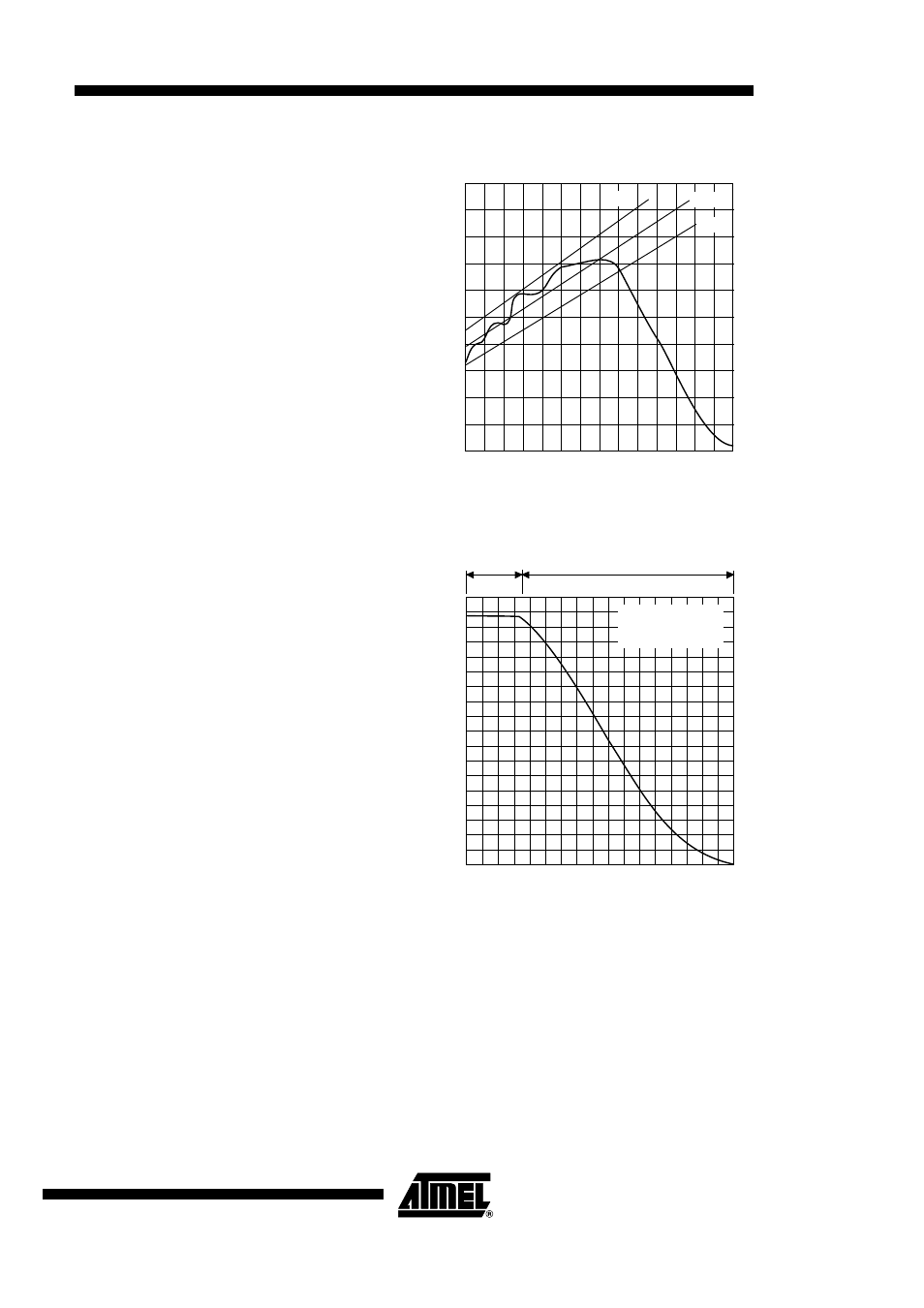
Figure 7. V
SAT
versus
Φ
A
Low Level Typical Curve
Exposure Time
Reduction (See
Figure 8)
TH7834 allows a reduction in the exposure time without changing the readout time. It
thus provides a function which is equivalent to an optical iris.
The exposure time reduction consists in increasing the
Φ
A
gate bias in order to remove
continuously, during period 2, the photoelectrons from the pixel and to inject them into
the antiblooming diode V
A
. When
Φ
A
returns to the normal bias, electrons are integrated
in the pixel.
Only excess electrons are evacuated into V
A
(blooming control). Thus, the actual inte-
gration time is ti instead of T
i
, without any change in the readout sequence. Register
transfer and reset clocks (
Φ
L
,
Φ
LS
and
Φ
R
) must be pulsed during the T
i
integration time.
4.0
4.8
5.6
6.4
7.2
8.0
3.2
2.4
1.6
0.8
400
500
600
700
800
900
1000
1100
Lambda (nm)
(V/
J/cm
2
)
µ
0
η
=0.8
η
=0.7
η
=0.6
1000
2400
1200
2600
1400
2800
3000
3200
3400
3600
Antiblooming
OFF
Antiblooming
ON
800
2200
600
2000
400
1800
200
1600
0
1
2
3
4
5
6
7
8 8.5
Φ
A bias (V)
Vsat.
(m
V)
0
VST = 4 V
R Low level = 1.5V
VA = 13V
Φ