Th7834c – Rainbow Electronics TH7834C User Manual
Page 8
8
TH7834C
1997A–IMAGE–05/02
Cross over of complementary clocks (
Φ
L1
and
Φ
L2
) preferably at 50% of their amplitude.
Note:
Generally, the difference between the floating diode level and signal level is the sum of
several signals:
• Register clock feedthrough
• Average CCD register dark signal proportional to CCD clock period, mode, temperature
• Pixel dark signal (depending upon temperature and exposure time)
• Pixel signal under illumination
Note:
1. Transients under 0.0V in the clock pulses will lead to charge injection, causing a localized increase of the dark signal. If such
spurious negative transients are present, they can be removed by inserting a serial resistor of appropriate value (typically
20
Ω
to 100
Ω
) at the relevant driver output.
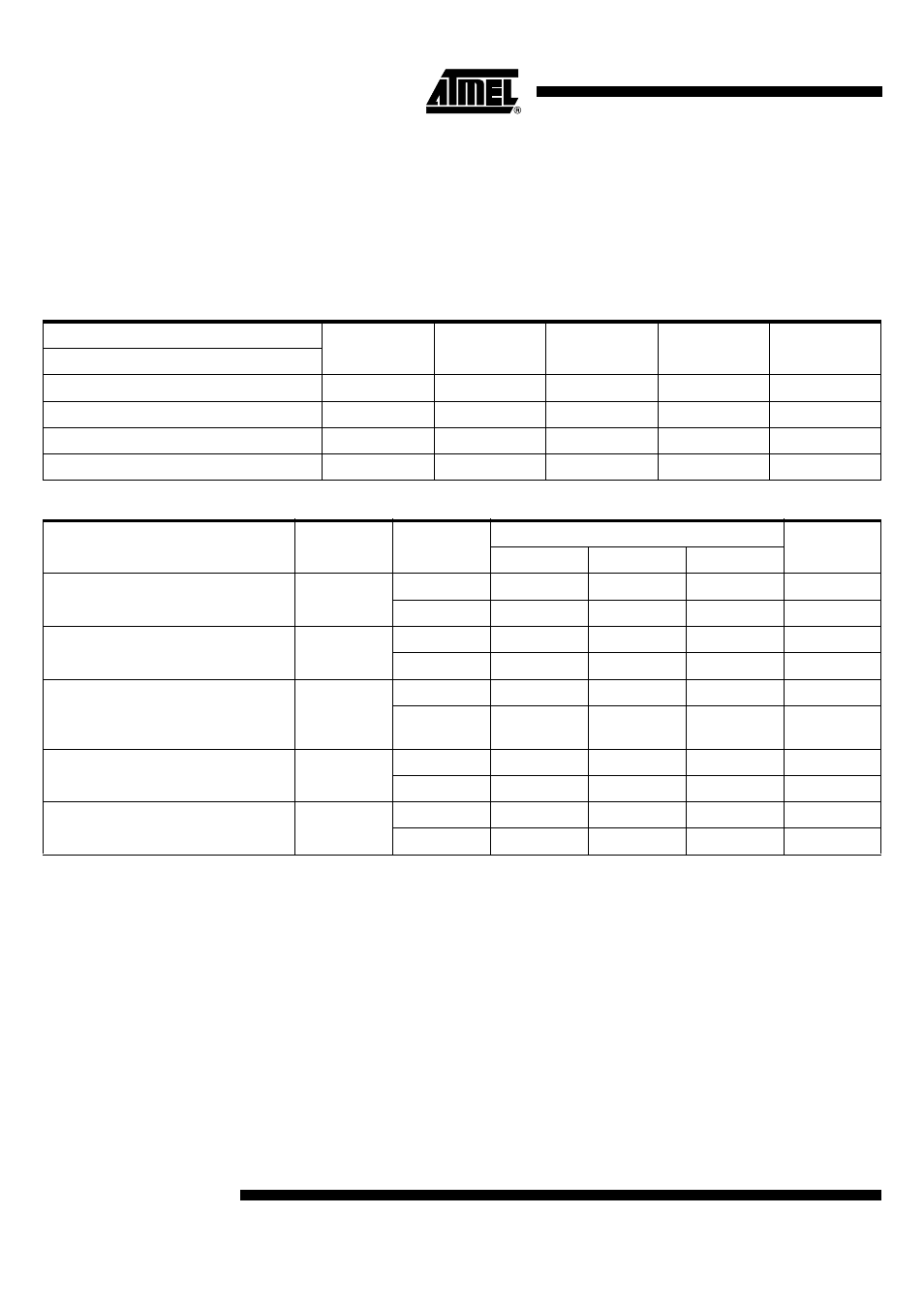
Table 2.
Elements
Inactive
Prescan
Dark
References
Isolation
Elements
Non Useful
Pixels
Useful Pixels
Signals
Register Clock Feedthrough
X
X
X
X
X
Average CCD Register Dark Signal
X
X
X
X
X
Pixel Dark Signal
X
X
X
Pixel Signal Under Illumination
X
X
Table 3. Drive Clock Voltage Swings
Parameter
Symbol
Logic
Value
Unit
Min.
Typ.
Max.
Register Main Transport Clock
Φ
L1
,
Φ
L2
High
8.5
9
11
V
Low
0
0.4
0.6
V
Register End Transport Clock
Φ
LS1-2
,
Φ
LS3-4
High
8.5
9
11
V
Low
0
0.2
0.4
V
Antiblooming (Low Level) And
Exposure Time Control (High Level)
Φ
A1-2
,
Φ
A3-4
High
9.5
10
10.5
V
Low
0
To be
adjusted
V
Reset Clock
Φ
R1-2
,
Φ
R3-4
High
10.5
11
12.5
V
Low
0
1.5
2
V
Transfer Clock
Φ
P1-2
,
Φ
P3-4
High
10.5
11
11.5
V
Low
0
0.4
0.6
V