Th7834c, Ls and, R). figure 2. driving schematic – Rainbow Electronics TH7834C User Manual
Page 4
4
TH7834C
1997A–IMAGE–05/02
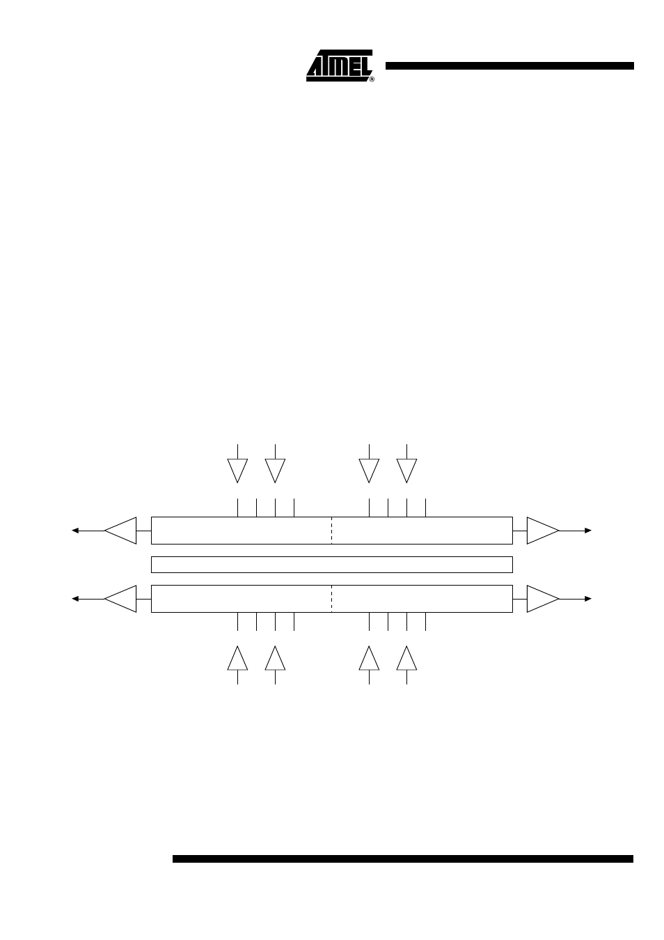
The four CCD shift registers have separated clocks. The output signal can be, then,
delivered simultaneously or sequentially on the four outputs.
The four CCD shift registers are designed with 4 separated gates. According to the gate
connection, the signal can be read through 2 or 4 output amplifiers.
According to gate connection, 2 or 4 output operating mode can be chosen. In the 4 out-
put operating mode, signals associated to the end pixels of the array (either pixels
number 1, 2 or pixels number 11999, 12000) are delivered first in time and signals corre-
sponding to the center of the line (pixels number 5999, 6000 and 6001, 6002) are
delivered last in time. Thus, external circuitry and processing are needed to combine the
four video outputs and to restore the normal order of the pixels in accordance with their
spatial distribution on the photosensitive line.
Terminal stages for every CCD shift register have separate clock control inputs in order
to speed up the final charge to voltage conversion and reduce the video output settling
time.
Antiblooming and exposure time control functions are provided.
Symmetrical TH7834 package PIN OUT allow to inverted pin 1 and 56 positions without
damage.
To obtain optimal operating mode, separated driving circuits are recommended for each
readout shift register (at least
Φ
LS and
Φ
R).
Figure 2. Driving Schematic
VOS1
VOS3
CCD A
CCD C
VOS2
VOS4
CCD B
2
6000
5999
6002
6001
11999
12000
1
Photosensitive line
CCD D
PHI3C
Pins
(1,2,3,4)B
Φ
Pins
(1,2,3,4)A
F
Pins
(1,2,3,4)D
Φ
Pins
(1,2,3,4)C
F
Φ
L1
Φ
L1
Φ
L1
Φ
L1
Logical signal :
Logical signal :
Logical signal :
Logical signal :
Φ
L2
Φ
L2
Φ
L2
Φ
L2