Rainbow Electronics RC1290 User Manual
Page 12
RC1240/1280/1290
2005 Radiocrafts AS
RC1240/RC1280/RC1290 Data Sheet (rev. 1.3)
Page 12 of 17
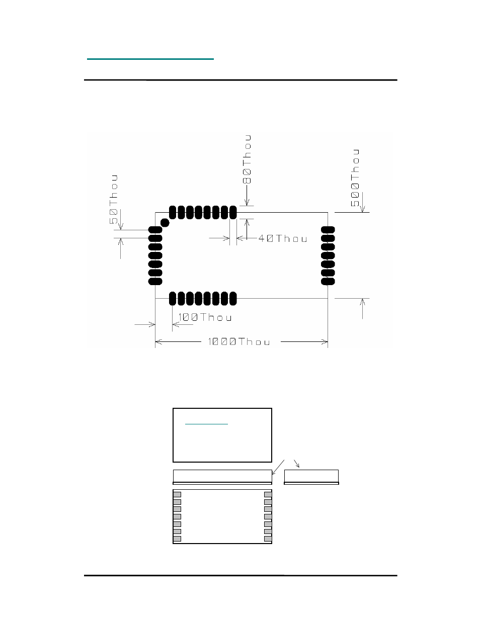
PCB Layout Recommendations
The recommended layout pads for the module are shown in the figure below. All dimensions
are in thousands of an inch (mil). The circle in upper left corner is an orientation mark only,
and should not be a part of the copper pattern.
The area underneath the module should be covered with solder resist in order to prevent
short circuiting the test pads on the back side of the module. A solid ground plane is
preferred. Unconnected pins should be soldered to the pads, and the pads should be left
floating.
Mechanical Drawing
RC10x0
CE
Top view
Side view
Bottom view
Shield can
End view
Drawings are not to scale
See also other documents in the category Rainbow Electronics Wireless Headsets:
- RC2000 (2 pages)
- Т7023 (12 pages)
- Т7024 (20 pages)
- RC2200 (17 pages)
- RF01 (26 pages)
- RC1090 (17 pages)
- U3741BM (32 pages)
- U3742BM (32 pages)
- RAM01 (7 pages)
- RF22 (92 pages)
- RC1180-MBUS (28 pages)
- RFM01 (8 pages)
- RF12B (36 pages)
- RC2300-ZNM (1 page)
- RF12 (31 pages)
- T48C862-R3 (107 pages)
- RF02 (24 pages)
- T48C862-R8 (107 pages)
- RFM12 (10 pages)
- U3745BM (29 pages)
- T5744 (19 pages)
- RFM12B (10 pages)
- U2745B (9 pages)
- T48C862-R4 (107 pages)
- RA01 (19 pages)
- T5754 (11 pages)
- U2741B (9 pages)
- RFM02 (8 pages)
- RC2100 (22 pages)
- RF модули диапазона ISM (4 pages)
- T5761 (35 pages)
- BTM -17х (5 pages)
- ATA8401 (12 pages)
- BTM -22х (7 pages)
- AT86RF231 (180 pages)
- ATA5575M1 (7 pages)
- AT88RF1354 (50 pages)
- ATA5812 (90 pages)
- AT86RF401 (50 pages)
- AT76C551 (77 pages)
- BTM -250 (6 pages)
- AT75C310 (132 pages)
- AT75C320 (13 pages)
- BTM -140 (6 pages)