Read cycle, Write cycle – Rainbow Electronics W24512A User Manual
Page 4
W24512A
- 4 -
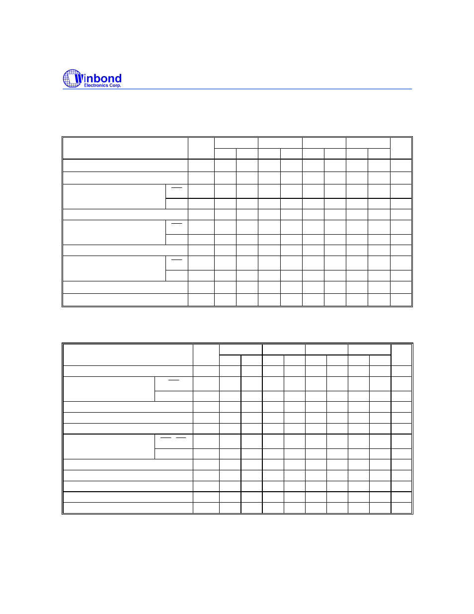
AC Characteristics, continued
(V
DD
= 5V
±
10%, V
SS
= 0V, T
A
= 0 to 70
°
C)
Read Cycle
PARAMETER
SYM.
W24512A-15
W24512A-25
W24512A-25
W24512A-35
UNIT
MIN.
MAX.
MIN.
MAX.
MIN.
MAX.
MIN.
MAX.
Read Cycle Time
T
RC
15
-
20
-
25
-
35
-
nS
Address Access Time
T
AA
-
15
-
20
-
25
-
35
nS
Chip Select Access Time
CS1
T
ACS1
-
15
-
20
-
25
-
35
nS
CS2
T
ACS2
-
15
-
20
-
25
-
35
nS
Output Enable to Output Valid
T
AOE
-
7
-
10
-
12
-
17
nS
Chip Selection to Output in Low Z
CS1
T
CLZ1*
3
-
3
-
3
-
3
-
nS
CS2
T
CLZ2*
3
-
3
-
3
-
3
-
nS
Output Enable to Output in Low Z
T
OLZ*
0
-
0
-
0
-
0
-
nS
Chip Deselection to Output in
CS1
T
CHZ1*
-
7
-
10
-
12
-
17
nS
High Z
CS2
T
CHZ2*
-
7
-
10
-
12
-
17
nS
Output Disable to Output in High Z
T
OHZ*
-
7
-
1
-
12
-
17
nS
Output Hold from Address Change
T
OH
3
-
3
-
3
-
3
-
nS
*
These parameters are sampled but not 100% tested.
Write Cycle
PARAMETER
SYM.
W24512A-15
W24512A-25
W24512A-25
W24512A-35
UNIT
MIN.
MAX.
MIN.
MAX.
MIN.
MAX.
MIN.
MAX.
Write Cycle Time
T
WC
15
-
20
-
25
-
35
-
nS
Chip Selection to End of Write
CS1
T
CW1
13
-
17
-
18
-
20
-
nS
CS2
T
CW2
13
-
17
-
18
-
20
-
nS
Address Valid to End of Write
T
AW
13
-
17
-
18
-
20
-
nS
Address Setup Time
T
AS
0
-
0
-
0
-
0
-
nS
Write Pulse Width
T
WP
10
-
12
-
15
-
18
-
nS
Write Recovery Time
CS1 , WE
T
WR1
0
-
0
-
0
-
0
-
nS
CS2
T
WR2
0
-
0
-
0
-
0
-
nS
Data Valid to End of Write
T
DW
9
-
10
-
12
-
15
-
nS
Data Hold from End of Write
T
DH
0
-
0
-
0
-
0
-
nS
Write to Output in High Z
T
WHZ*
-
8
-
10
-
12
-
15
nS
Output Disable to Output in High Z
T
OHZ*
-
8
-
10
-
12
-
15
nS
Output Active from End of Write
T
OW
0
-
0
-
0
-
0
-
nS
* T
hese parameters are sampled but not 100% tested.