Read cycle timing parameters, Byte/page-write cycle timing parameters – Rainbow Electronics W29EE011 User Manual
Page 11
W29EE011
Publication Release Date: July 1999
- 11 - Revision A12
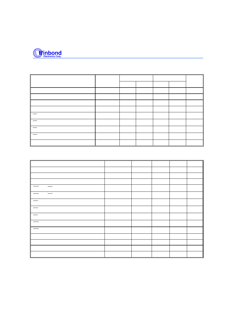
Read Cycle Timing Parameters
(V
CC
= 5.0V
±
10
%
, V
CC
= 5.0
±
5
%
for 70 nS, V
SS
= 0V, T
A
= 0 to 70
°
C)
PARAMETER
SYM.
W29EE011-90
W29EE011-15
UNIT
MIN.
MAX.
MIN.
MAX.
Read Cycle Time
T
RC
90
-
150
-
nS
Chip Enable Access Time
T
CE
-
90
-
150
nS
Address Access Time
T
AA
-
90
-
150
nS
Output Enable Access Time
T
OE
-
45
-
70
nS
CE
Low to Active Output
T
CLZ
0
-
0
-
nS
OE
Low to Active Output
T
OLZ
0
-
0
-
nS
CE
High to High-Z Output
T
CHZ
-
45
-
45
nS
OE
High to High-Z Output
T
OHZ
-
45
-
45
nS
Output Hold from Address Change
T
OH
0
-
0
-
nS
Byte/Page-write Cycle Timing Parameters
PARAMETER
SYMBOL
MIN.
TYP.
MAX.
UNIT
Write Cycle (Erase and Program)
T
WC
-
-
10
mS
Address Setup Time
T
AS
0
-
-
nS
Address Hold Time
T
AH
50
-
-
nS
WE and CE Setup Time
T
CS
0
-
-
nS
WE and CE Hold Time
T
CH
0
-
-
nS
OE High Setup Time
T
OES
10
-
-
nS
OE High Hold Time
T
OEH
10
-
-
nS
CE Pulse Width
T
CP
70
-
-
nS
WE Pulse Width
T
WP
70
-
-
nS
WE High Width
T
WPH
150
-
-
nS
Data Setup Time
T
DS
50
-
-
nS
Data Hold Time
T
DH
10
-
-
nS
Byte Load Cycle Time
T
BLC
0.22
-
200
µ
S
Byte Load Cycle Time-out
T
BLCO
300
-
-
µ
S
Note: All AC timing signals observe the following guidelines for determining setup and hold times:
(a) High level signal's reference level is V
IH
and (b) low level signal's reference level is V
IL
.