Rainbow Electronics MAX19998 User Manual
Page 3

SiGe, High-Linearity, 2300MHz to 4000MHz
Downconversion Mixer with LO Buffer
MAX19998
_______________________________________________________________________________________ 3
5.0V SUPPLY AC ELECTRICAL CHARACTERISTICS—fRF = 3100MHz to 3900MHz,
LOW-SIDE LO INJECTION
(Typical Application Circuit, with tuning elements outlined in Table 1, R1 = 698ω, R2 = 604ω, V
CC
= 4.75V to 5.25V, RF and LO ports
are driven from 50I sources, P
LO
= -3dBm to +3dBm, P
RF
= -5dBm, f
RF
= 3100MHz to 3900MHz, f
IF
= 300MHz, f
LO
= 2800MHz to
3600MHz, f
RF
> f
LO
, T
C
= -40NC to +85NC. Typical values are for T
C
= +25NC, V
CC
= 5.0V, P
RF
= -5dBm, P
LO
= 0dBm, f
RF
= 3500MHz,
f
LO
= 3200MHz, f
IF
= 300MHz. All parameters are guaranteed by design and characterization, unless otherwise noted.) (Note 7)
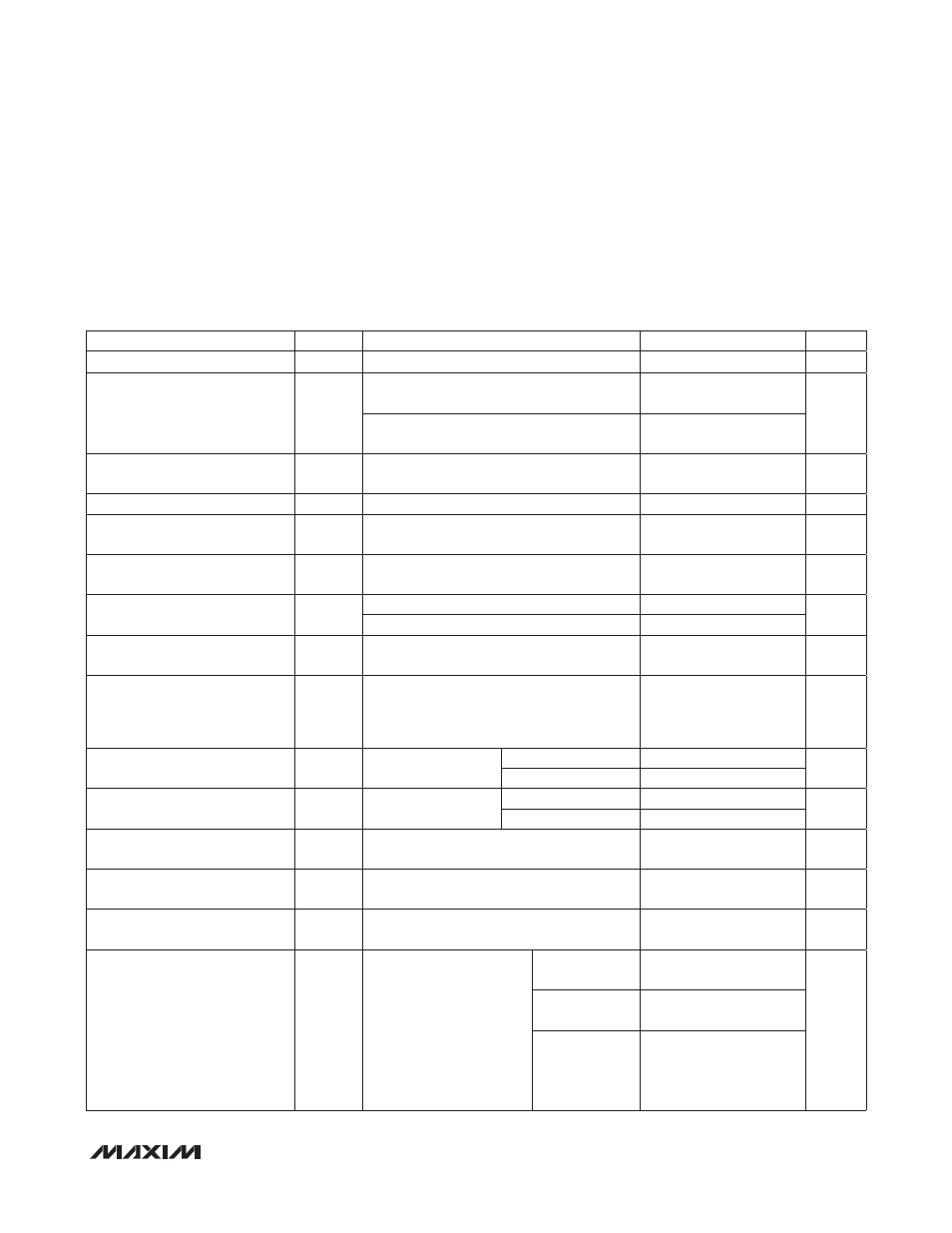
PARAMETER
SYMBOL
CONDITIONS
MIN
TYP
MAX
UNITS
Small-Signal Conversion Gain
G
C
T
C
= +25NC (Notes 8, 9)
7.6
8.7
9.4
dB
Gain Variation vs. Frequency
D
G
C
f
RF
= 3100MHz to 3900MHz, any 100MHz
band
0.15
dB
f
RF
= 3100MHz to 3900MHz, any 200MHz
band
0.3
Conversion Gain Temperature
Coefficient
TC
CG
f
RF
= 3100MHz to 3900MHz,
T
C
= -40NC to +85NC
-0.01
dB/NC
Input 1dB Compression Point
IP
1dB
(Note 10)
10.0
11.4
dBm
Third-Order Input Intercept Point
IIP3
f
RF1
- f
RF2
= 1MHz, P
RF1
= P
RF2
= -5dBm/tone,
T
C
= +25NC (Note 9)
22
24.3
dBm
IIP3 Variation with T
C
f
RF
= 3100MHz to 3900MHz, f
RF1
- f
RF2
= 1MHz,
P
RF1
= P
RF2
= -5dBm/tone, T
C
= -40NC to +85NC
Q
0.2
dBm
Single-Sideband Noise Figure
NF
SSB
No blockers present (Note 5)
9.7
12.5
dB
No blockers present, T
C
= +25NC (Note 5)
9.7
11.0
Noise Figure Temperature
Coefficient
TC
NF
Single sideband, no blockers present,
T
C
= -40NC to +85NC
0.018
dB/NC
Noise Figure Under Blocking
NF
B
+8dBm blocker tone applied to RF port,
f
RF
= 3500MHz, f
LO
= 3200MHz,
f
BLOCKER
= 3750MHz, P
LO
= 0dBm,
V
CC
= +5.0V, T
C
= +25NC (Notes 5, 11)
21
25
dB
2RF - 2LO Spur Rejection
2 x 2
f
SPUR
= f
LO
+ 150MHz
P
RF
= -10dBm (Note 5)
63
67
dBc
P
RF
= -5dBm (Note 9)
58
62
3RF - 3LO Spur Rejection
3 x 3
f
SPUR
= f
LO
+ 100MHz
P
RF
= -10dBm (Note 5)
80
85
dBc
P
RF
= -5dBm (Note 9)
70
75
RF Input Return Loss
RL
RF
LO on and IF terminated into a matched
impedance
25
dB
LO Input Return Loss
RL
LO
RF and IF terminated into a matched
impedance
16
dB
IF Output Impedance
Z
IF
Nominal differential impedance at the IC’s IF
outputs
200
I
IF Output Return Loss
RL
IF
RF terminated into 50I, LO
driven by 50I source, IF
transformed to 50I using
external components shown
in the Typical Application
Circuit. See the Typical
Operating Characteristics
for performance vs. inductor
values.
f
IF
= 450MHz,
L1 = L2 = 120nH
20
dB
f
IF
= 350MHz,
L1 = L2 = 270nH
20
f
IF
= 300MHz,
L1 = L2 = 390nH
20
