Rainbow Electronics MAX19998 User Manual
Page 24
SiGe, High-Linearity, 2300MHz to 4000MHz
Downconversion Mixer with LO Buffer
MAX19998
24 _____________________________________________________________________________________
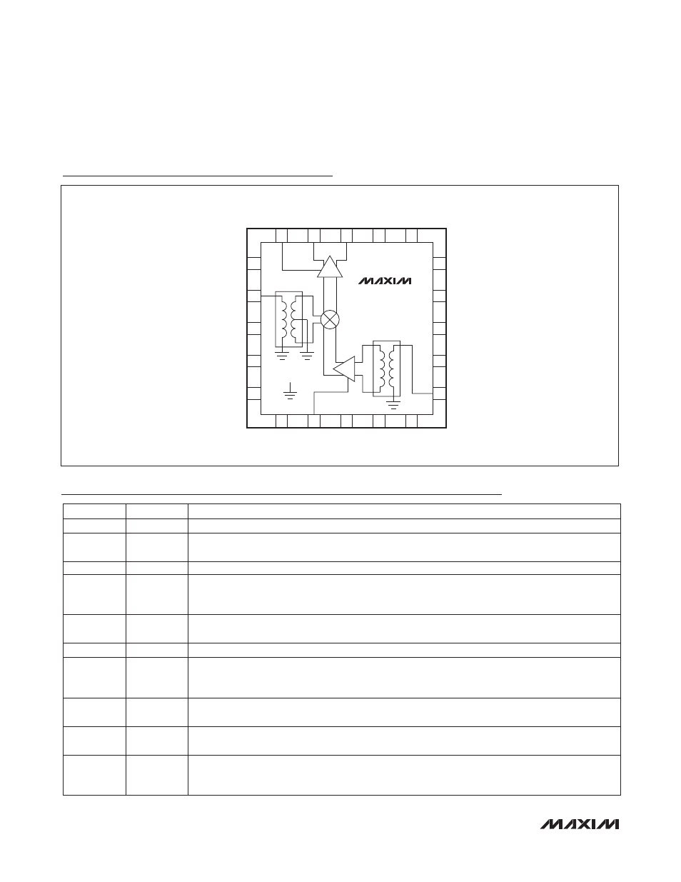
Pin Description
Pin Configuration/Functional Diagram
PIN
NAME
FUNCTION
1, 6, 8, 14
V
CC
Power Supply. Bypass to GND with 0.01FF capacitors as close as possible to the pin.
2
RF
Single-Ended 50I RF Input. Internally matched and DC shorted to GND through a balun. Provide an
input DC-blocking capacitor if required.
3, 9, 13, 15
GND
Ground. Not internally connected. Pins can be grounded.
4, 5, 10, 12,
17
GND
Ground. Internally connected to the exposed pad. Connect all ground pins and the exposed pad
(EP) together.
7
LOBIAS
LO Amplifier Bias Control. Output bias resistor for the LO buffer. Connect a 604I (5V, 230mA bias
condition) from LOBIAS to ground.
11
LO
Local Oscillator Input. This input is internally matched to 50I. Requires an input DC-blocking capacitor.
16
LEXT
External Inductor Connection. Connect a low-ESR 4.7nH inductor from this pin to ground to increase
the RF-to-IF and LO-to-IF isolation. Connect this pin directly to ground to reduce the component
count at the expense of reduced RF-to-IF and LO-to-IF isolation.
18, 19
IF-, IF+
Mixer Differential IF Output. Connect pullup inductors from each of these pins to V
CC
(see the Typical
Application Circuit).
20
IFBIAS
IF Amplifier Bias Control. IF bias resistor connection for the IF amplifier. Connect a 698I (5V, 230mA
bias condition) from IFBIAS to GND.
—
EP
Exposed Pad. Internally connected to GND. Solder this exposed pad to a PCB pad that uses multiple
ground vias to provide heat transfer out of the device into the PCB ground planes. These multiple via
grounds are also required to achieve the noted RF performance.
TOP VIEW
19
20
18
17
7
6
8
RF
GND
GND
9
V
CC
1
2
4
5
15
14
12
11
LOBIAS
V
CC
GND
GND
GND 3
13
16
10
V
CC
V
CC
GND
GND
LO
GND
IF+
IF-
GND
LEXT
IFBIAS
EP
MAX19998