Rainbow Electronics MAX5064 User Manual
Page 2
MAX5062/MAX5063/MAX5064
125V/2A, High-Speed,
Half-Bridge MOSFET Drivers
2
_______________________________________________________________________________________
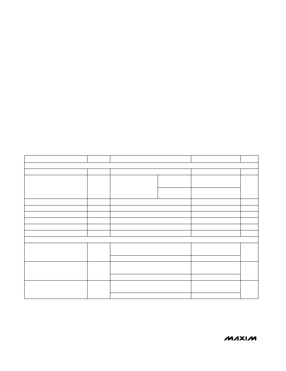
ABSOLUTE MAXIMUM RATINGS
ELECTRICAL CHARACTERISTICS
(V
DD
= V
BST
= +8V to +12.6V, V
HS
= GND = 0V, BBM = open, T
A
= -40°C to +125°C, unless otherwise noted. Typical values are at
V
DD
= V
BST
= +12V and T
A
= +25°C.) (Note 1)
Stresses beyond those listed under “Absolute Maximum Ratings” may cause permanent damage to the device. These are stress ratings only, and functional
operation of the device at these or any other conditions beyond those indicated in the operational sections of the specifications is not implied. Exposure to
absolute maximum rating conditions for extended periods may affect device reliability.
(All voltages referenced to GND, unless otherwise noted.)
V
DD
, IN_H, IN_L, IN_L+, IN_L-, IN_H+, IN_H-........-0.3V to +15V
DL, BBM .....................................................-0.3V to (V
DD
+ 0.3V)
HS............................................................................-5V to +130V
DH to HS.....................................................-0.3V to (V
DD
+ 0.3V)
BST to HS ...............................................................-0.3V to +15V
dV/dt at HS ........................................................................50V/ns
Continuous Power Dissipation (T
A
= +70°C)
8-Pin SO (derate 5.9mW/°C above +70°C)...............470.6mW
8-Pin SO With Exposed Pad (derate 19.2mW/°C
above +70°C)......................................................1538.5mW
12-Pin Thin QFN (derate 24.4mW/°C
above +70°C)......................................................1951.2mW
Maximum Junction Temperature .....................................+150°C
Operating Temperature Range .........................-40°C to +125°C
Storage Temperature Range .............................-65°C to +150°C
Lead Temperature (soldering, 10s) .................................+300°C
PARAMETER
SYMBOL
CONDITIONS
MIN
TYP
MAX
UNITS
POWER SUPPLIES
Operating Supply Voltage
V
DD
(Note 2)
8.0
12.6
V
MAX5062_/
MAX5063_
70
140
V
DD
Quiescent Supply Current
I
DD
IN_H = IN_L = GND
(no switching)
MAX5064_
120
260
µA
V
DD
Operating Supply Current
I
DDO
f
SW
= 500kHz, V
DD
= +12V
3
mA
BST Quiescent Supply Current
I
BST
IN_H = IN_L = GND (no switching)
15
40
µA
BST Operating Supply Current
I
BSTO
f
SW
= 500kHz, V
DD
= V
BST
= +12V
3
mA
UVLO (V
DD
to GND)
UVLO
VDD
V
DD
rising
6.5
7.3
8.0
V
UVLO (BST to HS)
UVLO
BST
BST rising
6.0
6.9
7.8
V
UVLO Hysteresis
0.5
V
LOGIC INPUT
MAX5062_/MAX5064A,
CMOS (V
DD
/ 2) version
0.67 x
V
DD
0.55 x
V
DD
Input-Logic High
V
IH_
MAX5063_/MAX5064B, TTL version
2
1.65
V
MAX5062_/MAX5064A,
CMOS (V
DD
/ 2) version
0.4 x
V
DD
0.33 x
V
DD
Input-Logic Low
V
IL_
MAX5063_/MAX5064B, TTL version
1.4
0.8
V
MAX5062_/MAX5064A,
CMOS (V
DD
/ 2) version
1.6
Logic-Input Hysteresis
V
HYS
MAX5063_/MAX5064B, TTL version
0.25
V