Rainbow Electronics MAX6965 User Manual
Page 9
Message Format for Reading
The MAX6965 is read using the MAX6965’s internally
stored command byte as an address pointer the same
way the stored command byte is used as an address
pointer for a write. The pointer autoincrements after
each data byte is read using the same rules as for a
write (Table 2). Thus, a read is initiated by first configur-
ing the MAX6965’s command byte by performing a
write (Figure 7). The master can now read n consecu-
tive bytes from the MAX6965 with the first data byte
being read from the register addressed by the initial-
ized command byte. When performing read-after-write
verification, remember to reset the command byte’s
address because the stored command byte address
has been autoincremented after the write (Table 2).
MAX6965
9-Output LED Driver with Intensity Control
_______________________________________________________________________________________
9
Figure 8. Command and Single Data Byte Received
S
A
A
A
P
0
SLAVE ADDRESS
COMMAND BYTE
DATA BYTE
1
BYTE
AUTOINCREMENT MEMORY ADDRESS
D15 D14 D13 D12 D11 D10
D9
D8
D1
D0
D3
D2
D5
D4
D7
D6
ACKNOWLEDGE FROM MAX
6965
ACKNOWLEDGE FROM MAX
6965
ACKNOWLEDGE FROM MAX
6965
HOW COMMAND BYTE AND DATA BYTE MAP INTO
MAX
6965
's REGISTERS
R/W
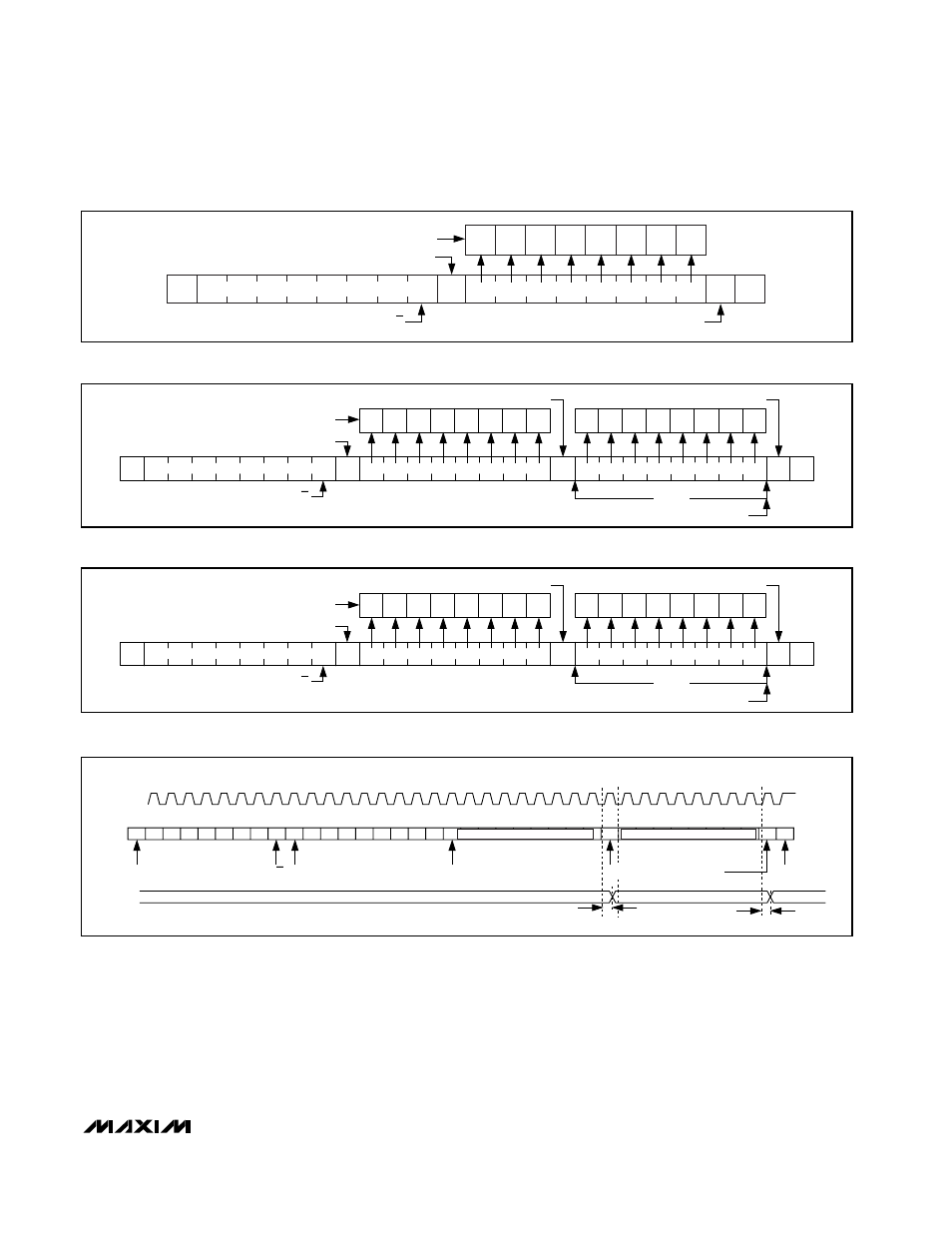
Figure 9. n Data Bytes Received
S
A
A
A
P
0
SLAVE ADDRESS
COMMAND BYTE
DATA BYTE
N
BYTES
D15 D14 D13 D12 D11 D10
D9
D8
D1
D0
D3
D2
D5
D4
D7
D6
ACKNOWLEDGE FROM MAX6965
ACKNOWLEDGE FROM MAX6965
ACKNOWLEDGE FROM MAX6965
HOW COMMAND BYTE AND DATA BYTE MAP INTO
MAX6965's REGISTERS
R/W
AUTOINCREMENT MEMORY ADDRESS
Figure 7. Command Byte Received
S
A
A
P
0
SLAVE ADDRESS
COMMAND BYTE
ACKNOWLEDGE FROM MAX6965
D15
D14
D13
D12
D11
D10
D9
D8
COMMAND BYTE IS STORED ON RECEIPT OF
STOP CONDITION
ACKNOWLEDGE FROM MAX6965
R/W
Figure 10. Write Timing Diagram
SLAVE ADDRESS
1
2
3
4
5
6
7
8
9
S A6 A5 A4 A3 A2 A1 A0
0
A
0
0
0
0
0
0
0
COMMAND BYTE
1
A
A
A
P
START CONDITION
ACKNOWLEDGE FROM SLAVE
ACKNOWLEDGE FROM SLAVE
ACKNOWLEDGE FROM SLAVE
STOP
CONDITION
O7–O0
DATA1 VALID
DATA2 VALID
t
DV
t
DV
SCL
SDA
WRITE TO OUTPUT PORTS REGISTERS (BLINK PHASE 0 REGISTERS/BLINK PHASE 1 REGISTERS)
R/W
MSB
LSB
DATA1
MSB
LSB
DATA2