Typical operating characteristics (continued), Pin description – Rainbow Electronics MAX6965 User Manual
Page 5
MAX6965
9-Output LED Driver with Intensity Control
_______________________________________________________________________________________
5
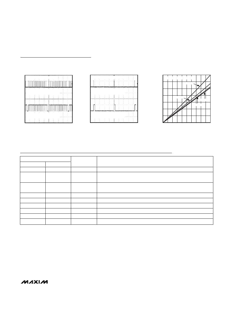
SCOPE SHOT OF TWO OUTPUT PORTS
MAX6965 toc07
2ms/div
OUTPUT 1
2V/div
OUTPUT 2
2V/div
MASTER INTENSITY SET TO 1/15
OUTPUT 1 INDIVIDUAL INTENSITY
SET TO 1/16
OUTPUT 2 INDIVIDUAL INTENSITY
SET TO 15/16
SCOPE SHOT OF TWO OUTPUT PORTS
MAX6965 toc08
2ms/div
OUTPUT 1
2V/div
OUTPUT 2
2V/div
OUTPUT 1 INDIVIDUAL INTENSITY
SET TO 1/16
MASTER INTENSITY SET TO 14/15
OUTPUT 2 INDIVIDUAL INTENSITY
SET TO 14/15
SINK CURRENT vs. V
OL
MAX6965 toc09
SINK CURRENT (mA)
V
OL
(V)
45
40
35
30
25
20
15
10
5
0.05
0.10
0.15
0.20
0.25
0.30
0.35
0
0
50
V+ = 3.3V
V+ = 3.6V
V+ = 2V
V+ = 2.7V
ONLY ONE OUTPUT LOADED
Typical Operating Characteristics (continued)
(T
A
= +25°C, unless otherwise noted.)
PIN
QSOP
QFN
NAME
FUNCTION
1
15
BLINK
Input Port. Configurable as blink control or general-purpose input.
2
16
RST
Reset Input. Active low clears the 2-wire interface and puts the device in same
condition as power-up reset.
3
1
AD0
Address Input. Sets device slave address. Connect to either GND, V+, SCL, or
SDA to give 4 logic combinations. See Table 1.
4–7, 9–13
2–5, 7–11
O0–O8
Output Ports. O0–O8 are open-drain outputs rated at 7V, 50mA.
8
6
GND
Ground. Do not sink more than 190mA into the GND pin.
14
12
SCL
I
2
C-Compatible Serial Clock Input
15
13
SDA
I
2
C-Compatible Serial Data I/O
16
14
V+
Positive Supply Voltage. Bypass V+ to GND with a 0.047µF ceramic capacitor
—
PAD
Exposed Pad
Exposed pad on packaged underside. Connect to GND.
Pin Description