Max6965, Output led driver with intensity control, C slave address map – Rainbow Electronics MAX6965 User Manual
Page 8: Table 2. register address map
MAX6965
during the high period of the clock pulse. When the
master is transmitting to the MAX6965, the device gen-
erates the acknowledge bit because the MAX6965 is
the recipient. When the MAX6965 is transmitting to the
master, the master generates the acknowledge bit
because the master is the recipient.
Slave Address
The MAX6965 has a 7-bit long slave address (Figure 6).
The eighth bit following the 7-bit slave address is the
R/W bit. The R/W bit is low for a write command, high
for a read command.
The second (A5), third (A4), fourth (A3), sixth (A1), and
last (A0) bits of the MAX6965 slave address are always
1, 0, 0, 0, and 0. Slave address bits A6 and A2 are
selected by the address input AD0. AD0 can be con-
nected to GND, V+, SDA, or SCL. The MAX6965 has
four possible slave addresses (Table 1), and therefore
a maximum of four MAX6965 devices can be controlled
independently from the same interface.
Message Format for Writing the MAX6965
A write to the MAX6965 comprises the transmission of
the MAX6965’s slave address with the R/W bit set to
zero, followed by at least 1 byte of information. The first
byte of information is the command byte. The command
byte determines which register of the MAX6965 is to be
written to by the next byte, if received (Table 2). If a
STOP condition is detected after the command byte is
received, then the MAX6965 takes no further action
beyond storing the command byte.
Any bytes received after the command byte are data
bytes. The first data byte goes into the internal register of
the MAX6965 selected by the command byte (Figure 8).
If multiple data bytes are transmitted before a STOP con-
dition is detected, these bytes are generally stored in
subsequent MAX6965 internal registers because the
command byte address autoincrements (Table 2). A
diagram of a write to the output ports registers (blink
phase 0 register or blink phase 1 register) is given in
Figure 10.
9-Output LED Driver with Intensity Control
8
_______________________________________________________________________________________
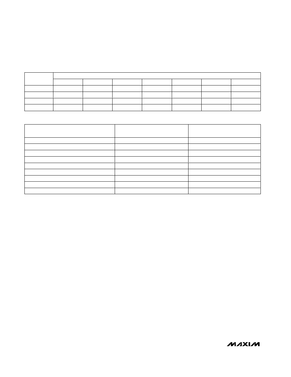
Table 1. MAX6965 I
2
C Slave Address Map
DEVICE ADDRESS
PIN AD0
A6
A5
A4
A3
A2
A1
A0
SCL
1
1
0
0
0
0
0
SDA
1
1
0
0
1
0
0
GND
0
1
0
0
0
0
0
V+
0
1
0
0
1
0
0
Table 2. Register Address Map
REGISTER
ADDRESS CODE
(hex)
AUTOINCREMENT
ADDRESS
Blink phase 0 outputs
0x01
0x01 (no change)
User RAM
0x03
0x03 (no change)
Blink phase 1 outputs
0x09
0x09 (no change)
Master, O8 intensity
0x0E
0x0E (no change)
Configuration
0x0F
0x0F (no change)
Outputs intensity O1, O0
0x10
0x11
Outputs intensity O3, O2
0x11
0x12
Outputs intensity O5, O4
0x12
0x13
Outputs intensity O7, O6
0x13
0x10