Absolute maximum ratings, Electrical characteristics – Rainbow Electronics MAX6965 User Manual
Page 2
MAX6965
9-Output LED Driver with Intensity Control
2
_______________________________________________________________________________________
ABSOLUTE MAXIMUM RATINGS
Stresses beyond those listed under “Absolute Maximum Ratings” may cause permanent damage to the device. These are stress ratings only, and functional
operation of the device at these or any other conditions beyond those indicated in the operational sections of the specifications is not implied. Exposure to
absolute maximum rating conditions for extended periods may affect device reliability.
Voltage (with respect to GND)
V+ .............................................................................-0.3V to +4V
SCL, SDA, AD0, BLINK, RST ...................................-0.3V to +6V
O0–O8 ......................................................................-0.3V to +8V
DC Current on O0 to O8 .....................................................55mA
DC Current on SDA.............................................................10mA
Maximum GND Current ....................................................190mA
Continuous Power Dissipation (T
A
= +70°C)
16-Pin QSOP (derate 8.3mW/°C over +70°C)..............666mW
16-Pin QFN (derate 14.7mW/°C over +70°C) ............1176mW
Operating Temperature Range (T
MIN
to T
MAX
) ...-40°C to +125°C
Junction Temperature ......................................................+150°C
Storage Temperature Range .............................-65°C to +150°C
Lead Temperature (soldering, 10s) .................................+300°C
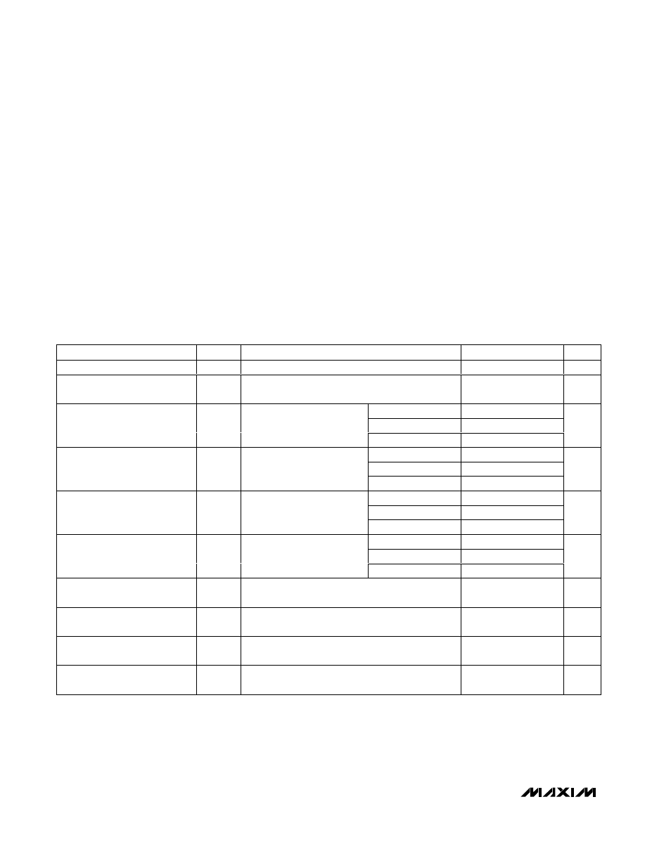
ELECTRICAL CHARACTERISTICS
(Typical Operating Circuit, V+ = 2V to 3.6V, T
A
= T
MIN
to T
MAX
, unless otherwise noted. Typical values are at V+ = 3.3V, T
A
= +25°C.)
(Note 1)
PARAMETER
SYMBOL
CONDITIONS
MIN
TYP
MAX
UNITS
Operating Supply Voltage
V+
2.0
3.6
V
Output Load External Supply
Voltage
V
EXT
0
7
V
T
A
= +25°C
1.2
2.3
T
A
= -40°C to +85°C
2.6
Standby Current
(Interface Idle, PWM Disabled)
I
+
S C L and S D A at V + ; other
d i g i tal i np uts at V + or GN D ;
P WM i ntensi ty contr ol d i sab l ed
T
A
= T
MIN
to T
MAX
3.3
µA
T
A
= +25°C
7
12.1
T
A
= -40°C to +85°C
13.3
Supply Current
(Interface Idle, PWM Enabled)
I
+
S C L and S D A at V + ; other
d i g i tal i np uts at V + or GN D ;
P WM i ntensi ty contr ol enab l ed
T
A
= T
MIN
to T
MAX
14.4
µA
T
A
= +25°C
40
76
T
A
= -40°C to +85°C
78
Supply Current
(Interface Running, PWM
Disabled)
I
+
f
SCL
= 400kHz; other digital
inputs at V+ or GND; PWM
intensity control disabled
T
A
= T
MIN
to T
MAX
80
µA
T
A
= +25°C
51
110
T
A
= -40°C to +85°C
117
Supply Current
(Interface Running, PWM
Enabled)
I
+
f
SCL
= 400kHz; other digital
inputs at V+ or GND; PWM
intensity control enabled
T
A
= T
MIN
to T
MAX
122
µA
Input High Voltage
SDA, SCL, AD0, BLINK, RST
V
IH
0.7
✕
V+
V
Input Low Voltage
SDA, SCL, AD0, BLINK, RST
V
IL
0.3
✕
V+
V
Input Leakage Current
SDA, SCL, AD0, BLINK, RST
I
IH
, I
IL
0
≤ input voltage ≤ 5.5V
-0.2
+0.2
µA
Input Capacitance
SDA, SCL, AD0, BLINK, RST
8
pF