Electrical characteristics (continued) – Rainbow Electronics MAX5475 User Manual
Page 3
MAX5471/MAX5472/MAX5474/MAX5475
32-Tap, Nonvolatile, Linear-Taper Digital
Potentiometers in SOT23
_______________________________________________________________________________________
3
Note 1: All devices are production tested at T
A
= +25°C and are guaranteed by design and characterization for -40°C < T
A
< +85°C.
Note 2: The DNL and INL are measured with the potentiometer configured as a variable resistor. For the 3-terminal potentiometers
(MAX5474/MAX5475), H is unconnected and L = GND. At V
DD
= 5.25V, W is driven with a source current of 80µA for the
50k
Ω configuration, and 40µA for the 100kΩ configuration. At V
DD
= 2.7V, the wiper terminal is driven with a source current
of 40µA for the 50k
Ω configuration, and 20µA for the 100kΩ configuration.
Note 3: The DNL and INL are measured with the potentiometer configured as a voltage-divider with H = V
DD
and L = GND
(MAX5474/MAX5475 only). The wiper terminal is unloaded.
Note 4: The wiper resistance is the worst value measured by injecting the currents given in Note 2 into W with L = GND.
R
W
= (V
W
- V
H
) / I
W
.
Note 5: The device draws higher supply current when digital inputs are driven with voltages between 0.3V x V
DD
and 0.7 x V
DD
.
Drive the digital inputs as close as possible to V
DD
or GND. (See the Typical Operating Characteristics for the Supply
Current vs. Digital Input Voltage graph.)
Note 6: Wiper at midscale with a 10pF load.
Note 7: Digital timing is guaranteed by design and characterization, and is not production tested.
Note 8: Wiper settling time is the worst-case 0% to 50% rise time measured between consecutive wiper positions. H = V
DD
, L =
GND, and the wiper terminal is unloaded and measured with a 10pF oscilloscope probe (see the Typical Operating
Characteristics for the Tap-to-Tap Switching Transient).
Note 9: Digital inputs CS, U/D, and INC are connected to GND or V
DD
. See the Typical Operating Characteristics for the Static
Supply Current vs. Temperature graph.
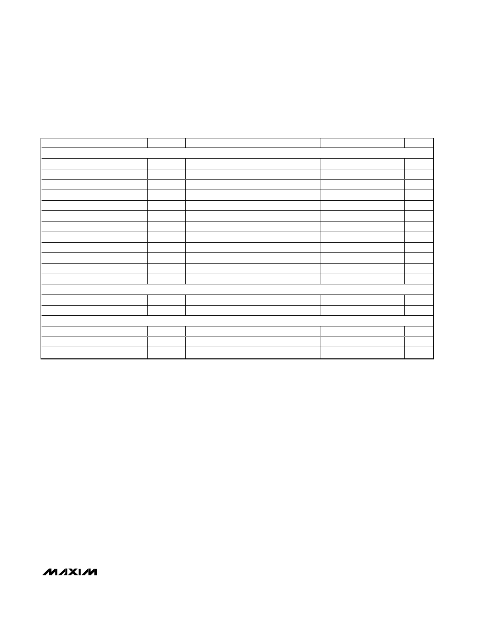
ELECTRICAL CHARACTERISTICS (continued)
(V
DD
= +2.7V to +5.25V, V
H
= V
DD
, V
L
= GND, T
A
= -40
°C to +85°C, unless otherwise noted. Typical values are at V
DD
= +5.0V, T
A
= +25
°C, unless otherwise noted.) (Note 1)
PARAMETER
SYMBOL
CONDITIONS
MIN
TYP
MAX
UNITS
TIMING CHARACTERISTICS (Figure 1, Note 7)
CS to INC Setup
t
CI
50
ns
INC High to U/D Change
t
ID
0
ns
U/D to INC Setup
t
DI
100
ns
INC Low Period
t
IL
50
ns
INC High Period
t
IH
50
ns
INC Cycle Time
t
CYC
100
ns
INC Inactive to CS Inactive
t
IC
100
ns
INC Active to CS Inactive
t
IK
100
ns
CS Deselect Time (Store)
t
CPH
100
ns
Wiper Settling Time
t
IW
(Note 8)
1
µs
Power-Up to Wiper Stable
t
PU
1
µs
Wiper Store Cycle
t
WSC
12
ms
NONVOLATILE MEMORY RELIABILITY
Data Retention
T
A
= +85°C
50
Year
Endurance
T
A
= +85°C
200,000
Store
POWER SUPPLY
Supply Voltage
V
DD
2.70
5.25
V
Supply Current
I
DD
Write to memory
400
µA
Static Supply Current
I
SD
T
A
= +25°C (Note 9)
0.35
1
µA