Typical operating characteristics (continued), Pin description – Rainbow Electronics MAX9729 User Manual
Page 9
MAX9729
Stereo Headphone Amplifier with BassMax,
Volume Control, and Input Mux
_______________________________________________________________________________________
9
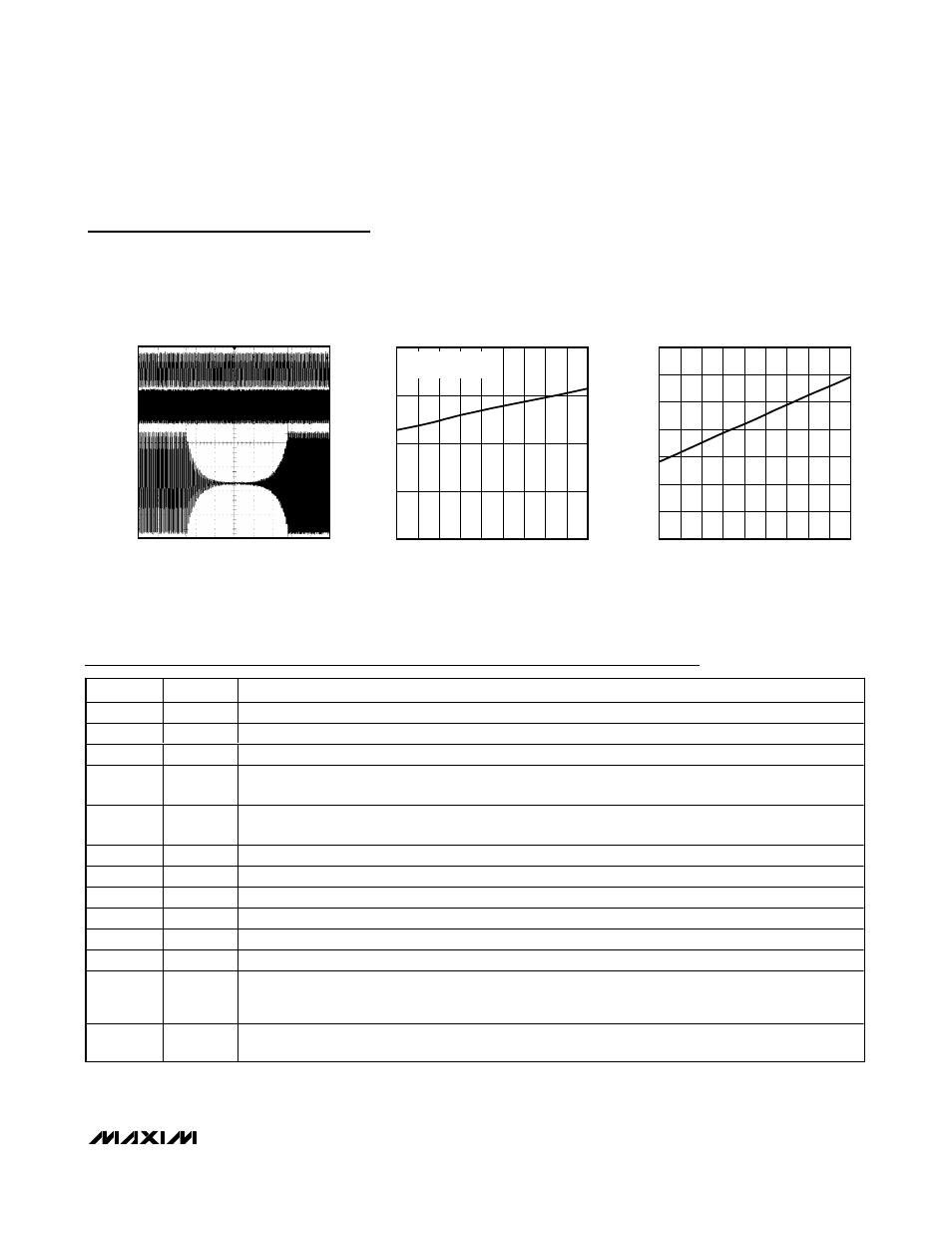
MAX9729 toc28
20ms/div
200mV/div
200mV/div
100mV/div
FADER OPERATION
SUPPLY CURRENT
vs. SUPPLY VOLTAGE
MAX9729 toc29
SUPPLY VOLTAGE (V)
SUPPLY CURRENT (mA)
3.4
3.2
3.0
2.8
2.6
2.4
2.2
2.0
3
4
5
6
2
1.8
3.6
NO LOAD
INPUTS AC-GROUNDED
SHUTDOWN CURRENT
vs. SUPPLY VOLTAGE
MAX9729 toc30
SUPPLY VOLTAGE (V)
SUPPLY CURRENT (
μ
A)
3.4
3.2
3.0
2.8
2.6
2.4
2.2
2.0
7
0
2
1
3
4
5
6
1.8
3.6
Typical Operating Characteristics (continued)
(V
DD
= PV
DD
=
SHDN = 3V, PGND = SGND = 0V, C1 = C2 = C3 = 1µF, C
IN
= 1µF (1206 case size, X7R dielectric ceramic capacitor),
BM_ = 0V, maximum gain setting = 3.5dB, volume attenuation setting = 0dB (total voltage gain = 3.5dB), BassMax disabled. Load
connected between OUT_ and PGND where specified. THD+N measurement BW = 22Hz to 22kHz. Both channels loaded and driven
in phase. T
A
= +25°C, unless otherwise noted.)
Pin Description
PIN
NAME
FUNCTION
1
INR2
Right-Channel Input 2
2
INR3
Right-Channel Input 3
3
SGND
Signal Ground. Connect SGND to PGND at a single point on the PCB near the device.
4, 8, 15,
22
N.C.
No Connection. Not internally connected.
5
ADD
Slave Address Selection Input. Connect ADD to V
DD
to set the device slave address to 1010001 or to
PGND to set the device slave address to 1010000.
6
PV
SS
Charge-Pump Output. Connect to SV
SS
.
7
SDA
Serial Data Input. Connect a pullup resistor greater than 500
Ω from SDA to PV
DD
.
9
C1N
Charge-Pump Flying Capacitor Negative Terminal. Connect a 1µF capacitor between C1P and C1N.
10
PGND
Power Ground. Connect PGND to SGND at a single point on the PCB near the device.
11
C1P
Charge-Pump Flying Capacitor Positive Terminal. Connect a 1µF capacitor between C1P and C1N.
12
SCL
Serial Clock Input. Connect a pullup resistor greater than 500
Ω from SCL to PV
DD
.
13
PV
DD
Charge-Pump and Logic Power-Supply Input. Bypass PV
DD
to PGND with a 1µF capacitor and connect
to V
DD
. PV
DD
and V
DD
are internally connected and should each have a 1µF bypass capacitor located
as close to the device as possible.
14
SV
SS
Headphone Amplifier Negative Power-Supply Input. Connect to PV
SS
and bypass with a 1µF capacitor
to PGND.