Max9729 – Rainbow Electronics MAX9729 User Manual
Page 22
MAX9729
Input-Coupling Capacitor
The AC-coupling capacitor (C
IN
) and input resistor (R
IN
)
form a highpass filter that removes any DC bias from an
input signal. See the
Functional Diagram/Typical
Operating Circuit
. C
IN
prevents any DC components
from the input signal source from appearing at the
amplifier outputs. The -3dB point of the highpass filter,
assuming zero source impedance due to the input sig-
nal source, is given by:
Choose C
IN
such that f
-3dB
is well below the lowest fre-
quency of interest. Setting f
-3dB
too high affects the
amplifier’s low-frequency response. Use capacitors with
low-voltage coefficient dielectrics. Aluminum electrolytic,
tantalum, or film dielectric capacitors are good choices
for AC-coupling capacitors. Capacitors with high-voltage
coefficients, such as ceramics (non-C0G dielectrics),
can result in increased distortion at low zero frequen-
cies. If a ceramic capacitor is selected due to board
space or cost constraints, use the largest package pos-
sible to minimize voltage coefficient effects. In addition,
use X7R dielectrics as opposed to X5R, Y5V, or Z5U.
BassMax Gain-Setting Components
The bass boost, low-frequency response when
BassMax is enabled, is set by the ratio of R1 to R2 (see
Figure 2), by the following equation:
where A
V_BOOST
is the gain boost, in dB, at low fre-
quencies. A
V_BOOST
is added to the gain realized by
the maximum gain setting and the volume setting. The
total gain at low frequencies is equal to:
where A
V_TOTAL_BM
is the total voltage gain at low fre-
quencies in dB, A
V_MAX
is the maximum gain setting in
dB, and ATTEN is the volume attenuation in dB. To
maintain circuit stability, the ratio:
must not exceed 1/2. A ratio equaling 1/3 is recommend-
ed. The switch that shorts BM_ to SGND, when BassMax
is disabled, can have an on-resistance as high as 300Ω.
Choose a value for R1 that is greater than 40kΩ to
ensure that positive feedback is negligible when
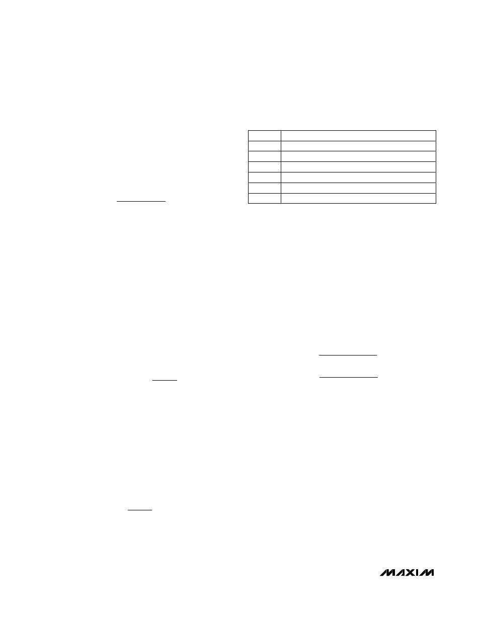
BassMax is disabled. Table 10 contains a list of R2 val-
ues, with R1 = 47kΩ, and the corresponding low-fre-
quency gain boost values.
The low-frequency boost attained by the BassMax cir-
cuit is added to the gain realized by the maximum gain
setting and volume setting. Select the BassMax gain so
that the output signal will remain within the dynamic
range of the MAX9729. Output signal clipping will occur
at low frequencies if the BassMax gain boost is exces-
sively large. See the
Output Dynamic Range
section.
Capacitor C4 forms a pole and a zero according to the
following equations:
f
POLE
is the frequency at which the gain boost begins
to roll off. f
ZERO
is the frequency at which the bass
boost gain no longer affects the transfer function. At
frequencies greater than or equal to f
ZERO
, the gain set
by the maximum gain setting and the volume control
attenuation dominate. Table 11 contains a list of capac-
itor values and the corresponding poles and zeros for a
given DC gain. See Figure 9 for an example of a gain
profile using BassMax.
Layout and Grounding
Proper layout and grounding are essential for optimum
performance. Connect PGND and SGND together at a
single point (star ground point) on the PCB near the
MAX9729. Connect PV
SS
and SV
SS
together at C2.
Place C2 physically close to PV
SS
and SV
SS
and con-
nect it to PGND. Bypass PV
DD
to PGND with C3.
Connect C3 as close to PV
DD
as possible. Bypass V
DD
to SGND with a 1µF capacitor. Place the V
DD
bypass
f
R
R
C
R
R
Hz
f
R
R
C
R
R
Hz
POLE
ZERO
=
−
Ч
Ч
Ч
=
+
Ч
Ч
Ч
1
2
2
6
1
2
1
2
2
6
1
2
π
π
(
)
(
)
R
R
R
2
1
2
+
A
A
ATTEN
A
dB
V TOTAL BM
V MAX
V BOOST
_
_
_
_
(
)
=
−
+
A
R
R
R
R
dB
V BOOST
_
log
(
)
=
×
+
−
20
1
2
1
2
f
R
C
Hz
dB
IN
IN
−
=
Ч
Ч
3
1
2
π
(
)
Stereo Headphone Amplifier with BassMax,
Volume Control, and Input Mux
22
______________________________________________________________________________________
R2 (k
Ω)
A
V_BOOST
(dB)
39
20.6
33
15.1
27
11.3
22
8.8
15
5.7
10
3.7
Table 10. BassMax Gain Examples,
R1 = 47kΩ