Applications information, Table 4. multiplexer/mixer control (register 0x00) – Rainbow Electronics MAX9729 User Manual
Page 17
Power-On Reset
The MAX9729 features internal power-on reset (POR)
circuitry that initializes the device upon power-up. The
contents of the MAX9729’s command registers at
power-on are shown in Table 9.
Applications Information
Power Dissipation and Heat Sinking
Linear power amplifiers can dissipate a significant
amount of power under normal operating conditions.
The maximum power dissipation for each package is
given in the
Absolute Maximum Ratings
section under
Continuous Power Dissipation or can be calculated by
the following equation:
where T
J(MAX)
is +150°C, T
A
is the ambient temperature,
and
θ
JA
is the reciprocal of the derating factor in °C/W as
specified in the
Absolute Maximum Ratings
section. For
example,
θ
JA
for the thin QFN package is +35°C/W.
If the power dissipation exceeds the rated package
dissipation, reduce V
DD
, increase load impedance,
decrease the ambient temperature, or add heatsinking.
Large output, supply, and ground traces decrease
θ
JA
,
allowing more heat to be transferred from the package
to surrounding air.
Output Dynamic Range
Dynamic range is the difference between the noise
floor of the system and the output level at 1% THD+N. It
is essential that a system’s dynamic range be known
before setting the maximum output gain. Output clip-
ping will occur if the output signal is greater than the
dynamic range of the system. The DirectDrive architec-
ture of the MAX9729 has increased dynamic range (for
a given V
DD
) compared to other single-supply ampli-
fiers. Due to the absolute maximum ratings of the
MAX9729 and to limit power dissipation, the MAX9729
includes internal circuitry that limits the output voltage
to approximately ±2.5V.
Use the THD+N vs. Output Power graph in the
Typical
Operating Characteristics
to identify the system’s
dynamic range. Find the output power that causes 1%
THD+N for a given load. This point will indicate what
output power causes the output to begin to clip. Use
the following equation to determine the peak-to-peak
output voltage that causes 1% THD+N for a given load:
where P
OUT_1%
is the output power that causes 1%
THD+N, R
L
is the load resistance, and V
OUT_(P-P)
is the
peak-to-peak output voltage. Determine the total volt-
age gain (A
V_TOTAL
) necessary to attain this output
voltage based on the maximum peak-to-peak input
voltage (V
IN_(P-P)
):
The A
V_TOTAL
setting is determined by the maximum
voltage gain setting, volume setting, and bass boost
gain if BassMax is enabled (see the
Maximum Gain
Control, Volume Control, and BassMax Gain-Setting
Components
sections).
UVLO
The MAX9729 features an undervoltage lockout (UVLO)
function that prevents the device from operating if the
supply voltage is less than 1.65V. This feature ensures
proper operation during brownout conditions and pre-
vents deep battery discharge. Once the supply voltage
exceeds the UVLO threshold, the MAX9729 charge
pump is turned on, the amplifiers are powered (provid-
ed that
SHDN is high), and the command registers are
reset to their POR values (see Table 9).
Component Selection
Charge-Pump Capacitor Selection
Use ceramic capacitors with a low ESR for optimum perfor-
mance. For optimal performance over the extended tem-
perature range, select capacitors with an X7R dielectric.
A
V
V
V TOTAL
OUT P P
IN P P
_
_(
)
_(
)
=
−
−
V
P
R
OUT P P
OUT
L
_(
)
_ %
(
)
−
=
×
2 2
1
P
T
T
D MAX
J MAX
A
JA
(
)
(
)
=
−
θ
MAX9729
Stereo Headphone Amplifier with BassMax,
Volume Control, and Input Mux
______________________________________________________________________________________
17
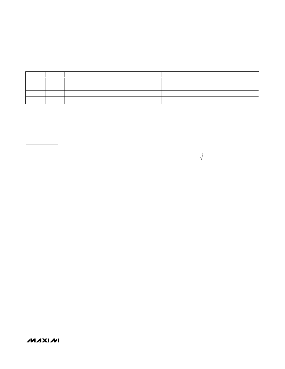
B6
B5
OUTL
OUTR
0
0
INL1 x A
V_TOTAL
INR1 x A
V_TOTAL
0
1
INL2 x A
V_TOTAL
INR2 x A
V_TOTAL
1
0
INL3 x A
V_TOTAL
INR3 x A
V_TOTAL
1
1
(INL1 + INL2 + INL3) x A
V_TOTAL
(INR1 + INR2 + INR3) x A
V_TOTAL
Table 4. Multiplexer/Mixer Control (Register 0x00)