Rainbow Electronics MAX9729 User Manual
Page 2
MAX9729
Stereo Headphone Amplifier with BassMax,
Volume Control, and Input Mux
2
_______________________________________________________________________________________
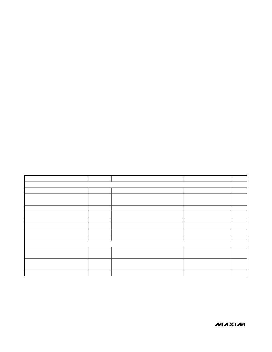
ABSOLUTE MAXIMUM RATINGS
ELECTRICAL CHARACTERISTICS (3V Supply)
(V
DD
= PV
DD
=
SHDN = 3V, PGND = SGND = 0V, C1 = C2 = C3 = 1µF, BM_ = 0V, maximum gain setting = 6dB, volume attenuation
setting = -16dB (overall gain = -10dB), BassMax disabled. Load connected between OUT_ and PGND where specified. THD+N
measurement BW = 22Hz to 22kHz. T
A
= T
MIN
to T
MAX
, unless otherwise noted. Typical values are at T
A
= +25°C.) (Note 1)
Stresses beyond those listed under “Absolute Maximum Ratings” may cause permanent damage to the device. These are stress ratings only, and functional
operation of the device at these or any other conditions beyond those indicated in the operational sections of the specifications is not implied. Exposure to
absolute maximum rating conditions for extended periods may affect device reliability.
V
DD
, PV
DD
to PGND or SGND .................................-0.3V to +4V
V
DD
to PV
DD
................................................Internally Connected
PV
SS
to SV
SS
.......................................................................±0.3V
SGND to PGND...................................................................±0.3V
C1P to PGND..............................................-0.3V to (V
DD
+ 0.3V)
C1N to PGND............................................(PV
SS
- 0.3V) to +0.3V
PV
SS
, SV
SS
to PGND ................................................+0.3V to -4V
INL_, INR_, BEEP to SGND............(SV
SS
- 0.3V) to (V
DD
+ 0.3V)
SDA, SCL, BEEP_EN to PGND.................................-0.3V to +4V
SHDN to PGND ..........................................-0.3V to (V
DD
+ 0.3V)
OUT_ to PGND ............................................................-3V to +3V
BM_ to SGND ..............................................................-2V to +2V
Duration of OUT_ Short Circuit to PGND....................Continuous
Continuous Current Into/Out of:
V
DD
, C1P, C1N, PGND, PV
SS
, SV
SS
, or OUT_ .............±0.85A
All other pins.................................................................±20mA
Continuous Power Dissipation (T
A
= +70°C, multilayer board)
28-Pin Thin QFN (derate 28.6mW/°C above +70°C) 0.2286mW
Junction-to-Ambient Thermal Resistance (
θ
JA
)
28-Pin TQFN.................................................................35°C/W
Operating Temperature Range ...........................-40°C to +85°C
Junction Temperature ......................................................+150°C
Storage Temperature Range .............................-65°C to +150°C
OUT_ ESD Protection (Human Body Model) .......................±8kV
ESD Protection of All Other Pins ..........................................±2kV
Lead Temperature (soldering, 10s) .................................+300°C
PARAMETER
SYMBOL
CONDITIONS
MIN
TYP
MAX
UNITS
GENERAL
Supply Voltage Range
V
DD
(Note 2)
1.8
3.6
V
Charge-Pump and Logic Supply
Voltage
PV
DD
(Note 2)
1.8
3.6
V
Quiescent Supply Current
I
DD
No load, BEEP_EN = V
DD
(Note 3)
5.5
8
mA
Shutdown Supply Current
I
DD_SHDN
V
SHDN
= 0V
5
10
µA
Turn-On Time
t
ON
From shutdown mode to full operation
200
µs
Beep Enable Time
t
ON_BEEP
12
µs
Thermal Shutdown Threshold
T
THRES
146
°C
Thermal Shutdown Hysteresis
T
HYST
13
°C
HEADPHONE AMPLIFIER
Input Resistance
R
IN
Applicable to all maximum gain and
volume settings
14
25
35
k
Ω
Output Offset Voltage
V
OSHP
Measured between OUT_ and SGND,
overall gain = -10dB (Note 3)
±0.7
±3.5
mV
BMR, BML Input Bias Current
I
BIAS_BM
±10
±100
nA