Threshold – Xilinx V2.1 User Manual
Page 95

Math
95
Xilinx Blocks
64. This corresponds to one CLB per output bit. If the table depth is greater than 64, a
quarter wave is stored, and additional logic is used to generate the remaining portions
of the wave. Storing only the quarter wave for the large tables reduces the area
needed. Block memory stores a full wave for all table depths and widths that can be
implemented in a single block memory. Otherwise, values are stored as a quarter
wave. Latency for the distributed ROM implementation is determined by the input
width, whether or not the block is pipelined, and the given latency value.
The minimum pipeline for block ROM implementations is 1, thus the minimum
latency is 1. The maximum latency for block ROM is also 1 except for the cases
outlined in the table below.
The Core datasheet can be found on your local disk at:
%XILINX%\coregen\ip\xilinx\primary\com\xilinx\ip\sincos_v3_0\d
oc\C_SIN_COS_V3_0.pdf
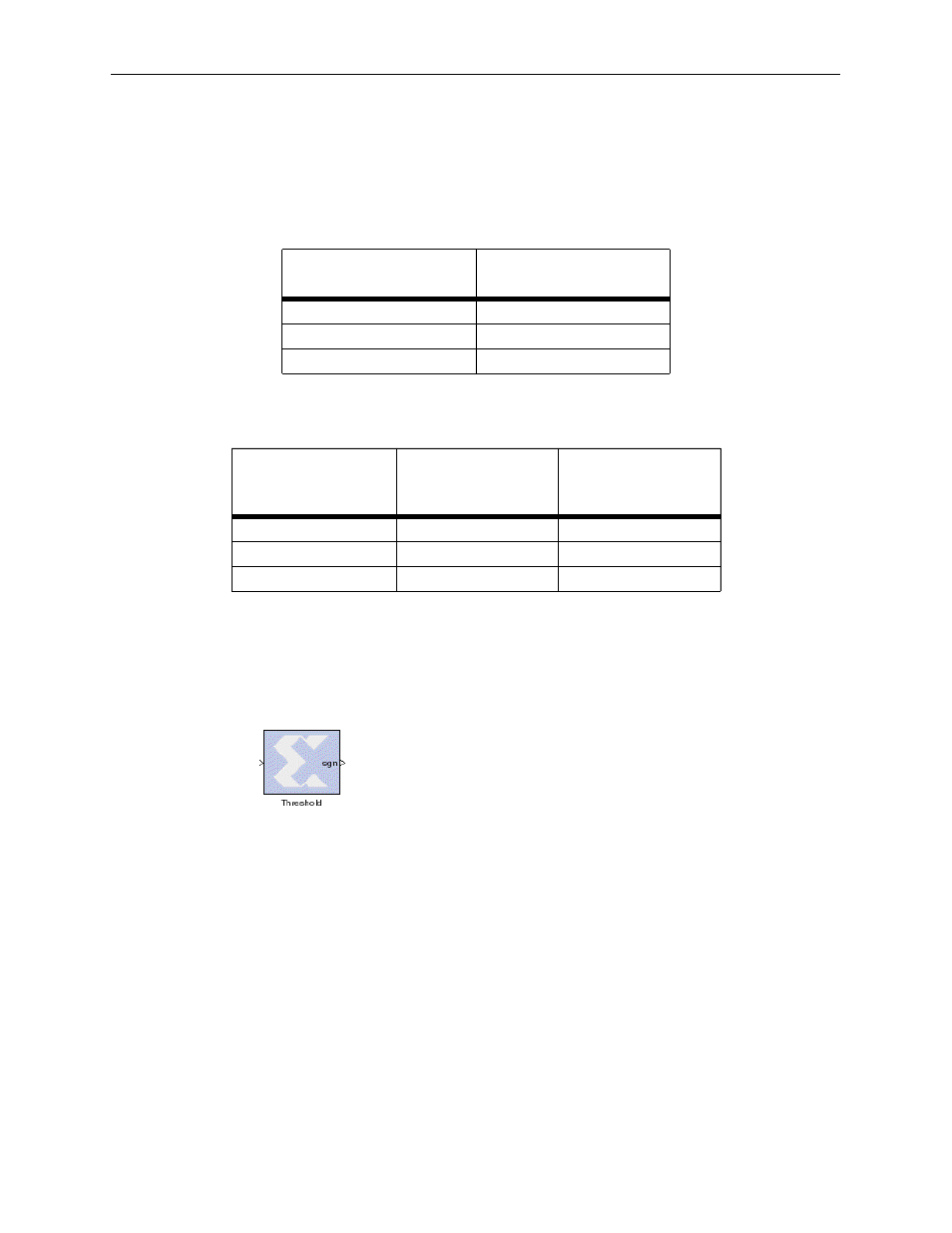
Threshold
The Xilinx Threshold block tests the sign of the input number. If the
input number is negative, the output of the block is -1; otherwise, the
output is 1. The output is a signed fixed point integer that is 2 bits
long. The block has one input and one output.
Input Width
Block Latency Range using
Distributed ROM
3-6
1-2
7-8
1-4
9-10
1-5
Input Width
Output Width
Maximum Core
Latency Using Block
ROM
Greater than 10
Greater than 16
2
Equal to 10
Greater than 4
2
Greater than 9
Greater than 8
2
