Up sample – Xilinx V2.1 User Manual
Page 50

50
Xilinx Development System
Xilinx System Generator v2.1 Reference Guide
added to the channel that is last to present a valid input sample. Note that if this
parameter is zero, the block has a feed-through path; otherwise, it does not.
Other parameters used by this block are described in the Common Parameters section
of a previous chapter in this manual.
The Xilinx Sync block does not use a Xilinx LogiCORE.
Up Sample
The Xilinx Up Sample block increases the sample rate at the point
where the block is placed in your design. The input signal is over-
sampled so that every nth input sample is presented at the output, or
presented once with (n-1) zeroes interspersed.
The output sample period is i/k, where i is the input sample period
and k the sampling rate.
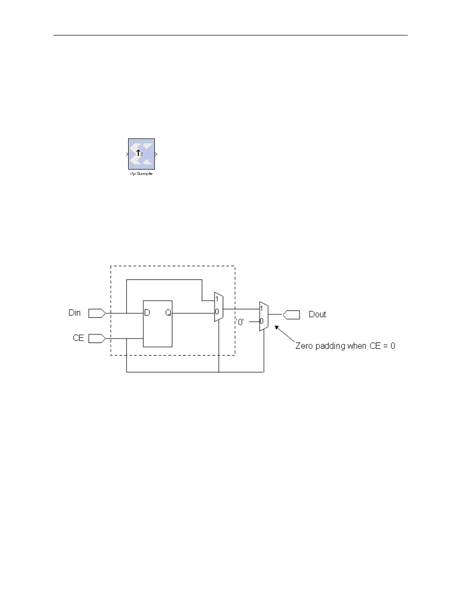
In Simulink, a block changes its output right after it is enabled. In hardware, a
register does not change until the clock enable is sampled, i.e. one clock cycle later. To
make the hardware cycle-true to the Simulink model, the up sample block is
implemented with the circuit shown below. The portion of the circuit within the
dashed line is always present. The additional mux used for zero padding is removed
if the
Copy Samples
option is selected on the block parameters dialog box.
Figure 3-27: Up sample block hardware implementation
The clock enable connected to this circuit is the same one that is distributed to the
blocks connected to its input. The timing diagram shown below demonstrates the
circuit's behavior. It is important to notice that this circuit has a combinatorial path
