Down sample – Xilinx V2.1 User Manual
Page 36

36
Xilinx Development System
Xilinx System Generator v2.1 Reference Guide
Down Sample
The Xilinx Down Sample block reduces the sample rate at the point
where the block is placed in your design. The input signal is under-
sampled so that every nth input sample is presented at the output and
held.
Output sample period is
ki,
where
k
is the sampling rate and
i
is
the input sample period.
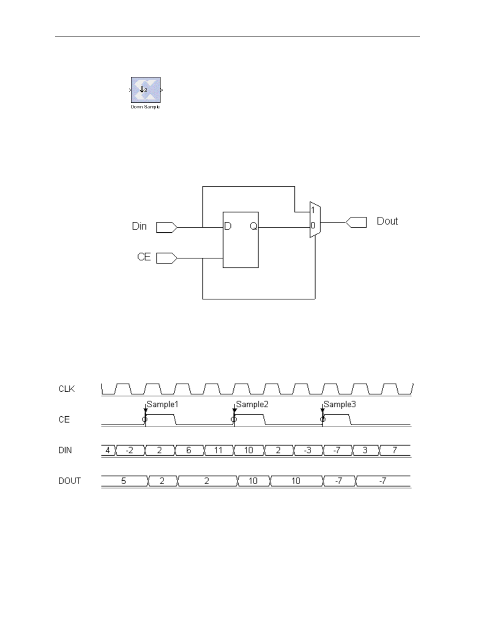
In Simulink, a block changes its output right after it is enabled. In hardware, a
register does not change until the clock enable is sampled, i.e. one clock cycle later. To
make the hardware cycle-true to the Simulink model, the down sample block is
implemented with the following circuit in hardware:
Figure 3-10: Hardware implementation of down sample block
The clock enable connected to this circuit is the same one that is distributed to the
blocks connected to its output. The timing diagram shown below demonstrates the
circuit's behavior. It is important to notice that this circuit has a combinatorial path
from
din
to
dout
. Whenever possible put a register or delay block after a down
sample block.
Figure 3-11: Down sample circuit behavior
