Power management, Table 1-29, Ac adapter and 12v input power jack/switch – Xilinx SP605 User Manual
Page 55: For details on
SP605 Hardware User Guide
55
UG526 (v1.8) September 24, 2012
Detailed Description
19. Power Management
AC Adapter and 12V Input Power Jack/Switch
The SP605 is powered from a 12V source that is connected through a 6-pin (2X3) right angle
Mini-Fit type connector J18. The AC-to-DC power supply included in the kit has a mating
6-pin plug.
When the SP605 is installed into a table top or tower PC's PCIe slot, the SP605 is typically
powered from the PC ATX power supply. One of the PC’s ATX hard disk type 4-pin power
connectors is plugged into SP605 connector J27. The SP605 can be powered with the AC
power adapter (plugged into J18) even when plugged into a PC PCIe motherboard slot;
G21
FMC_LA20_P
R9
H20
FMC_LA15_N
D19
G22
FMC_LA20_N
R8
H22
FMC_LA19_P
R11
G24
FMC_LA22_P
V7
H23
FMC_LA19_N
T11
G25
FMC_LA22_N
W8
H25
FMC_LA21_P
V11
G27
FMC_LA25_P
W14
H26
FMC_LA21_N
W11
G28
FMC_LA25_N
Y14
H28
FMC_LA24_P
AA14
G30
FMC_LA29_P
T15
H29
FMC_LA24_N
AB14
G31
FMC_LA29_N
U15
H31
FMC_LA28_P
AA16
G33
FMC_LA31_P
U16
H32
FMC_LA28_N
AB16
G34
FMC_LA31_N
V15
H34
FMC_LA30_P
Y15
G36
FMC_LA33_P
Y17
H35
FMC_LA30_N
AB15
G37
FMC_LA33_N
AB17
H37
FMC_LA32_P
W17
H38
FMC_LA32_N
Y18
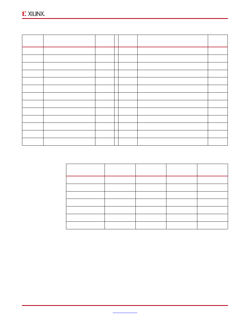
Table 1-28:
VITA 57.1 FMC LPC Connections (Cont’d)
J63 FMC
LPC Pin
Schematic Net Name
U1 FPGA
Pin
J63 FMC
LPC Pin
Schematic Net Name
U1 FPGA
Pin
Table 1-29:
Power Supply Voltages for LPC Connector
Voltage Supply
Voltage
Number
of Pins
Maximum
Current
Tolerance
VADJ
Fixed 2.5V
2
2A
±5%
VIO_B_M2C
NC
0
0A
N/A
VREF_A_M2C
0-VADJ
1
0.001A
±2%
VREF_B_M2C
NC
0
0A
N/A
3P3VAUX
3.3V
1
0.020A
± 5%
3P3V
3.3V
4
3A
±5%
12P0V
12V
2
1A
±5%