Pci express endpoint connectivity, Table 1-11, Updated – Xilinx SP605 User Manual
Page 31
SP605 Hardware User Guide
31
UG526 (v1.8) September 24, 2012
Detailed Description
9. PCI Express Endpoint Connectivity
The 1-lane PCIe edge connector performs data transfers at the rate of 2.5 GT/s for a Gen1
application. The Spartan-6 FPGA GTP MGT is used for the multi-gigabit per second serial
interface.
The SP605 board trace impedance on the PCIe lane supports Gen1 applications. The SP605
supports Gen1 x1.
The PCIe interface obtains its power from the DC power supply provided with the SP605
or through the 12V ATX power supply connector. The PCIe edge connector is not used for
any power connections.
The board can be powered by one of two 12V sources; J18, a 6-pin (2x3) Mini-Fit-type
connector and J27, a 4-pin (inline) ATX disk drive type connector.
The 6-pin Mini-Fit-type connector provides 60W (12V @ 5A) from the AC power adapter
provided with the board while the 4-pin ATX disk drive type connector is provided for
users who want to power their board while it is installed inside a PC chassis.
For applications requiring additional power, such as the use of expansion cards drawing
significant power, a larger AC adapter might be required. If a different AC adapter is used,
its load regulation should be better than ±10%.
SP605 power slide switch SW2 turns the board on and off by controlling the 12V supply to
the board.
Caution!
Caution! Never apply power to the power brick 6-pin Mini-Fit type connector (J18)
and the 4-pin ATX disk drive type connector (J27) at the same time as this will result in damage
to the board. Never connect an auxiliary PCIe 6-pin power connector to J18 6-pin Mini-Fit type
connector on the SP605 board as this could result in damage to the PCIe motherboard and/or
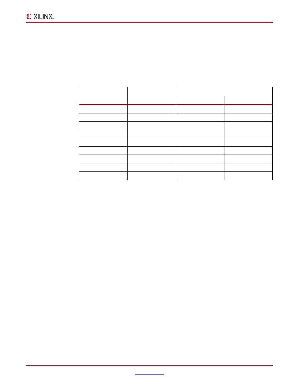
Table 1-11:
PCIe Edge Connector Connections
U1 FPGA Pin
Schematic Net Name
P4 PCIe Edge Connector
Pin Number
Pin Name
C7
PCIE_RX0_N
B15
PETn0
D7
PCIE_RX0_P
B14
PETp0
A6
PCIE_TX0_N
(1)
A17
PERn0
B6
PCIE_TX0_P
(1)
A16
PERp0
–
PCIE_CLK_QO_N
(2)
A14
REFCLK-
–
PCIE_CLK_QO_P
(2)
A13
REFCLK+
B10
PCIE_250M_N
(3)(6)
U48.17
(4)
NQ
A10
PCIE_250M_P
(3)(6)
U48.18
(4)
Q
J7
PCIE_PERST_B_LS
A11
PERST
(5)
Notes:
1. Each of the TX0_N/P signals has a 0.1 µF series capacitor.
2. PCIE_CLK_QO_N/P is the PC motherboard 100MHZ REFCLK.
3. Each of the PCIE_250M_N/P signals has a 0.1 µF series capacitor.
4. U48 is an ICS874001 clock multiplier device (U48.17/18 are not P4 pins).
5. The PERST signal from pin P4.A11 is isolated by a series resistor and then level-shifted by U52 before
making the FPGA pin U1.J7 connection.
6. PCIE_250M_N/P signals can be a frequency other than 250 MHz, depending on the settings selected
by resistor population for U48 ICS874001. The default setting is 125 MHz.