User sip header, Detailed description, Table 1-26: user sip header connections – Xilinx SP605 User Manual
Page 47
SP605 Hardware User Guide
47
UG526 (v1.8) September 24, 2012
Detailed Description
User SIP Header
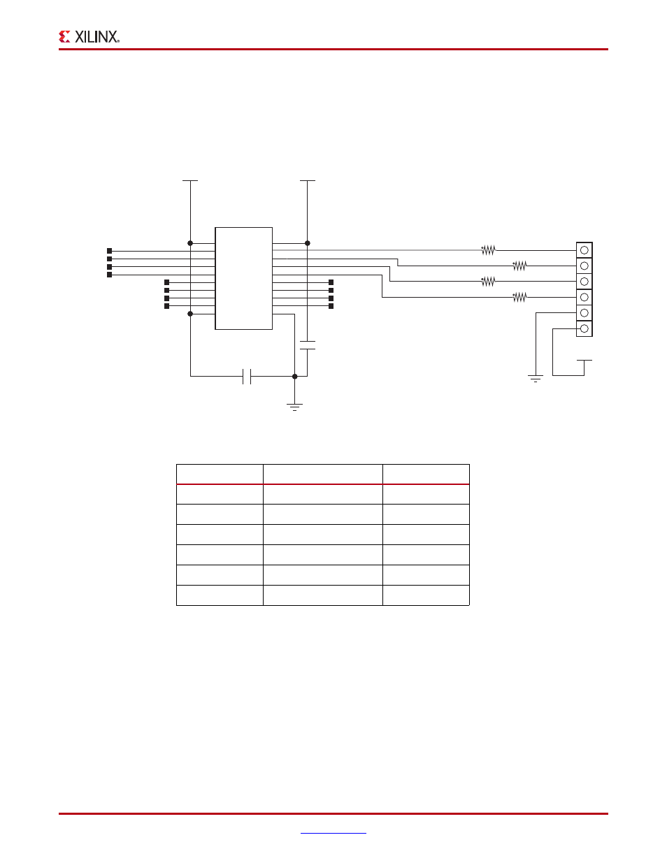
The SP605 includes a 6-pin single-inline (SIP) male pin header (J55) for FPGA GPIO access.
Four pins of J55 are wired to the FPGA through 200
Ω series resistors and a level shifter, and
the remaining two J55 pins are wired to 3.3V and GND. The J55 header is described in
X-Ref Target - Figure 1-18
Figure 1-18:
User SIP Header J55
VCC3V3
HDR_1x6
GPIO_HEADER_3
GPIO_HEADER_2
GPIO_HEADER_1
GPIO_HEADER_0
2
1
5%
1/16W
200
R2
8
1
1
2
R2
8
0
200
1/16W
5%
1
2
3
4
5
6
J55
DNP
1
2
R2
8
2
200
1/16W
5%
2
1
5%
1/16W
200
R2
8
3
TXB0108
VCCB
B1
B2
B3
B4
B6
B7
GND
A3
A8
OE
A4
A5
A7
A6
B5
A1
A2
B8
VCCA
VCC1V5_FPGA
VCC3V3
GPIO_HEADER_0
GPIO_HEADER_1
GPIO_HEADER_2
GPIO_HEADER_3
GPIO_HEADER_0_LS
GPIO_HEADER_1_LS
NC
NC
NC
NC
2
12
3
1
15
7
8
6
5
10
9
4
11
13
14
16
17
18
20
19
U52
1
2
X5R
10V
0.1UF
C3
8
5
2
1
C384
0.1UF
10V
X5R
NC
NC
NC
NC
GPIO_HEADER_2_LS
GPIO_HEADER_3_LS
U1 FPGA Pin
G7
H6
D1
R7
UG526_18 _092409
Table 1-26:
User SIP Header Connections
U1 FPGA Pin
Schematic Net Name
GPIO Header Pin
G7
GPIO_HEADER_0
J55.1
H6
GPIO_HEADER_1
J55.2
D1
GPIO_HEADER_2
J55.3
R7
GPIO_HEADER_3
J55.4
–
GND
J55.5
–
VCC3V3
J55.6
Notes:
1. Each GPIO_HEADER_n signal is sourced from the FPGA as
<netname>_LS to a level shifter, then to the J55 header.
2. Each GPIO_HEADER_n net has a 200
Ω series resistor between the
level shifter and its respective header pin.