Cc2420 – Texas Instruments 3138 155 232931 User Manual
Page 79

CC2420
SWRS041B Page 79 of 89
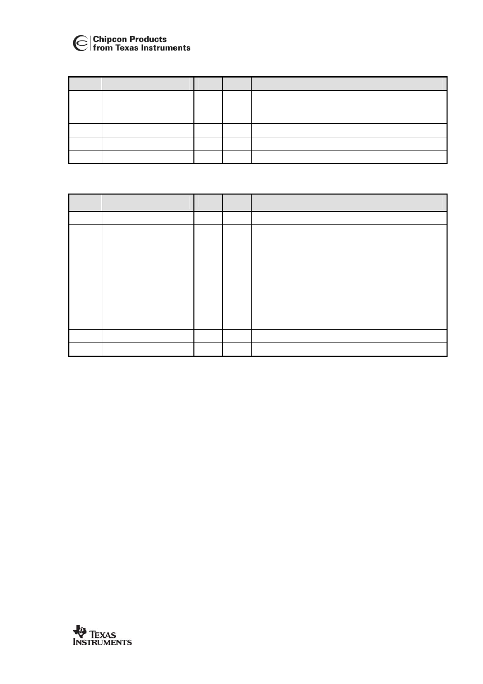
ADCTST (0x2D) - ADC Test Register
Bit
Field Name
Reset
R/W
Description
15 ADC_CLOCK_DISABLE
0 R/W
ADC Clock Disable
0 : Clock enabled when ADC enabled
1 : Clock disabled, even if ADC is enabled
14:8 ADC_I[6:0]
0
R
Read the current ADC I-branch value.
7 -
0
W0
Reserved, write as 0.
6:0 ADC_Q[6:0]
0 R
Read the current ADC Q-branch value.
DACTST (0x2E) - DAC Test Register
Bit
Field Name
Reset
R/W
Description
15 -
0 W0
Reserved, write as 0.
14:12 DAC_SRC[2:0]
0
R/W
The TX DACs data source is selected by DAC_SRC according
to:
0: Normal operation (from modulator).
1: The DAC_I_O and DAC_Q_O override values below.-
2: From ADC, most significant bits
3: I/Q after digital down mixing and channel filtering.
4: Full-spectrum White Noise (from CRC)
5: From ADC, least significant bits
6: RSSI / Cordic Magnitude Output
7: HSSD module.
This feature will often require the DACs to be manually turned on
in MANOR and TOPTST.ATESTMOD_MODE=4.
11:6 DAC_I_O[5:0]
0
R/W
I-branch DAC override value.
5:0 DAC_Q_O[5:0]
0 R/W
Q-branch DAC override value.
