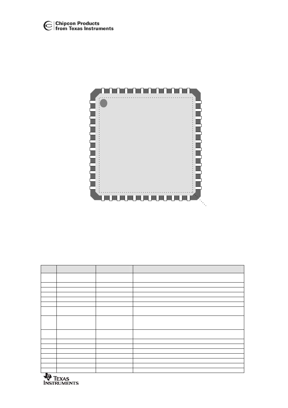
Pin assignment, Cc2420, 7 pin assignment – Texas Instruments 3138 155 232931 User Manual
Page 15: Qlp48 7x7

CC2420
SWRS041B Page 15 of 89
7 Pin
Assignment
VR
E
G
_
O
U
T
A
V
DD_
CHP
QLP48
7x7
1
2
3
4
5
6
7
8
9
10
11
12
35
34
33
32
31
30
29
28
27
26
25
36
13
14
15
16
17
18
19
20
21
22
23
24
48
47
46
45
44
43
42
41
40
39
38
37
CC2420
R_BIAS
A
V
DD_
IF1
VR
E
G
_
IN
VR
E
G
_
E
N
X
O
SC
16_Q1
X
O
SC
16_Q2
A
T
EST2
A
T
EST1
NC
RF_P
RF_N
AVDD_PRE
AVDD_RF1
TXRX_SWITCH
AVDD_VCO
VCO_GUARD
AVDD_SW
GND
GND
NC
NC
DS
UB
_
C
ORE
DS
UB
_
P
A
D
S
AVD
D
_
AD
C
DV
DD_
A
D
C
DGUA
RD
A
V
DD_
IF2
DGND_
GUA
R
D
A
V
DD_
RF2
DGND
NC
CSn
FIFO
FIFOP
CCA
SFD
DVDD1.8
SCLK
DVDD_RAM
SI
SO
DVDD3.3
NC
A
V
D
D
_
XOSC
16
NC
AGND
Exposed die
attach pad
R
ESETn
Figure 1.
CC2420 Pinout – Top View
Pin
Pin Name
Pin type
Pin Description
-
AGND
Ground (analog)
Exposed die attach pad. Must be connected to solid ground
plane
1
VCO_GUARD
Power (analog)
Connection of guard ring for VCO (to AVDD) shielding
2
AVDD_VCO
Power (analog)
1.8 V Power supply for VCO
3
AVDD_PRE
Power (analog)
1.8 V Power supply for Prescaler
4
AVDD_RF1
Power (analog)
1.8 V Power supply for RF front-end
5
GND
Ground (analog)
Grounded pin for RF shielding
6
RF_P
RF I/O
Positive RF input/output signal to LNA/from PA in
receive/transmit mode
7
TXRX_SWITCH
Power (analog)
Common supply connection for integrated RF front-end. Must
be connected to RF_P and RF_N externally through a DC
path
8
RF_N
RF I/O
Negative RF input/output signal to LNA/from PA in
receive/transmit mode
9
GND
Ground (analog)
Grounded pin for RF shielding
10
AVDD_SW
Power (analog)
1.8 V Power supply for LNA / PA switch
11
NC
- Not
Connected
12
NC
- Not
Connected
13
NC
- Not
Connected
14
AVDD_RF2
Power (analog)
1.8 V Power supply for receive and transmit mixers
15
AVDD_IF2
Power (analog)
1.8 V Power supply for transmit / receive IF chain
