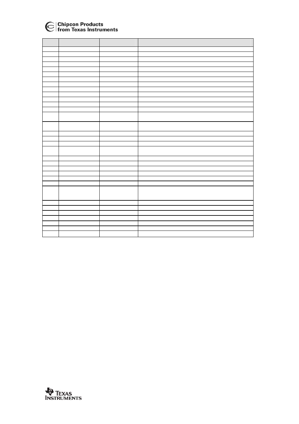
Cc2420 – Texas Instruments 3138 155 232931 User Manual
Page 16

CC2420
SWRS041B Page 16 of 89
Pin
Pin Name
Pin type
Pin Description
16
NC
- Not
Connected
17
AVDD_ADC
Power (analog)
1.8 V Power supply for analog parts of ADCs and DACs
18
DVDD_ADC
Power (digital)
1.8 V Power supply for digital parts of receive ADCs
19
DGND_GUARD
Ground (digital)
Ground connection for digital noise isolation
20
DGUARD
Power (digital)
1.8 V Power supply connection for digital noise isolation
21
RESETn
Digital Input
Asynchronous, active low digital reset
22
DGND
Ground (digital)
Ground connection for digital core and pads
23
DSUB_PADS
Ground (digital)
Substrate connection for digital pads
24
DSUB_CORE
Ground (digital)
Substrate connection for digital modules
25
DVDD3.3
Power (digital)
3.3 V Power supply for digital I/Os
26
DVDD1.8
Power (digital)
1.8 V Power supply for digital core
27
SFD
Digital output
SFD (Start of Frame Delimiter) / digital mux output
28
CCA
Digital output
CCA (Clear Channel Assessment) / digital mux output
29
FIFOP
Digital output
Active when number of bytes in FIFO exceeds threshold /
serial RF clock output in test mode
30
FIFO
Digital I/O
Active when data in FIFO /
serial RF data input / output in test mode
31
CSn
Digital input
SPI Chip select, active low
32
SCLK
Digital input
SPI Clock input, up to 10 MHz
33
SI
Digital input
SPI Slave Input. Sampled on the positive edge of SCLK
34
SO
Digital output
(tristate)
SPI Slave Output. Updated on the negative edge of SCLK.
Tristate when CSn high.
35
DVDD_RAM
Power (digital)
1.8 V Power supply for digital RAM
36
NC
- Not
Connected
37
AVDD_XOSC16
Power (analog)
1.8 V crystal oscillator power supply
38
XOSC16_Q2
Analog I/O
16 MHz Crystal oscillator pin 2
39
XOSC16_Q1
Analog I/O
16 MHz Crystal oscillator pin 1 or external clock input
40
NC
- Not
Connected
41
VREG_EN
Digital input
Voltage regulator enable, active high, held at VREG_IN
voltage level when active. Note that VREG_EN is relative
VREG_IN, not DVDD3.3.
42
VREG_OUT
Power output
Voltage regulator 1.8 V power supply output
43
VREG_IN
Power (analog)
Voltage regulator 2.1 to 3.6 V power supply input
44
AVDD_IF1
Power (analog)
1.8 V Power supply for transmit / receive IF chain
45
R_BIAS
Analog output
External precision resistor, 43 k
Ω, ± 1 %
46
ATEST2
Analog I/O
Analog test I/O for prototype and production testing
47
ATEST1
Analog I/O
Analog test I/O for prototype and production testing
48
AVDD_CHP
Power (analog)
1.8 V Power supply for phase detector and charge pump
NOTES:
The exposed die attach pad must be connected to a solid ground plane as this is the main ground connection for the
chip.
