Section 4.3 – Texas Instruments TMS320DM646X DMSOC User Manual
Page 52
Registers
www.ti.com
4.3
Asynchronous n Configuration Registers (A1CR-A4CR)
The asynchronous configuration register (ACFGn) is used to configure the shaping of the address and
control signals during an access to asynchronous memory. It is also used to program the width of
asynchronous interface and to select from various modes of operation. This register can be written prior to
any transfer, and any asynchronous transfer following the write will use the new configuration. The ACFGn
is shown in
and described in
. There are four ACFGns. Each chip select space has a
dedicated ACFGn. This allows each chip select space to be programmed independently to interface to
different asynchronous memory types.
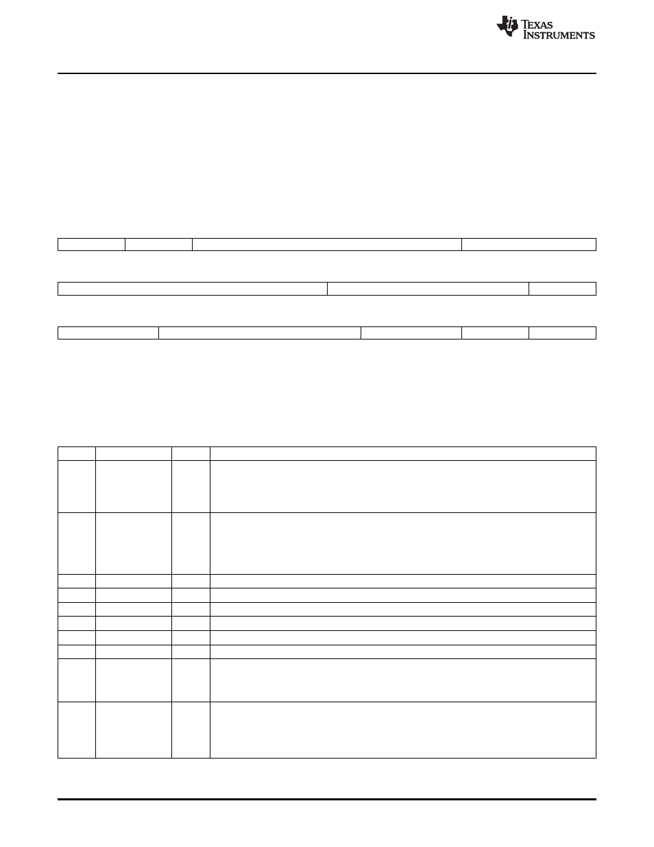
Figure 22. Asynchronous n Configuration Register (ACFGn)
31
30
29
26
25
24
SS
EW
(A)
W_SETUP
W_STROBE
(B)
R/W-0
R/W-0
R/W-Fh
R/W-3Fh
23
20
19
17
16
W_STROBE
(B)
W_HOLD
R_SETUP
R/W-3Fh
R/W-7h
R/W-Fh
15
13
12
7
6
4
3
2
1
0
R_SETUP
R_STROBE
(B)
R_HOLD
TA
ASIZE
R/W-Fh
R/W-3Fh
R/W-7h
R/W-3h
R/W-0
LEGEND: R/W = Read/Write; -n = value after reset
A. The EW bit must be cleared to 0 when operating in NAND Flash mode.
B. The W_STROBE and R_STROBE bits must not be cleared to 0 when operating in Extended Wait mode.
Table 35. Asynchronous n Configuration Register (ACFGn) Field Descriptions
Bit
Field
Value
Description
31
SS
Select Strobe bit. This bit defines whether the asynchronous interface operates in Normal mode or
Select Strobe mode. See
for details on the two modes of operation.
0
Normal mode is enabled.
1
Select Strobe mode is enabled.
30
EW
Extend Wait enable bit. This bit enables extended wait cycles. See
on extended wait
cycles for details. This bit must be cleared to 0, if the EMIF on your device does not have a
EM_WAIT pin.
0
Extended wait cycles are disabled.
1
Extended wait cycles are enabled.
29-26
W_SETUP
0-Fh
Write setup width in EMIF clock cycles, minus 1 cycle. See
for details.
25-20
W_STROBE
0-3Fh
Write strobe width in EMIF clock cycles, minus 1 cycle. See
for details.
19-17
W_HOLD
0-7h
Write hold width in EMIF clock cycles, minus 1 cycle. See
for details.
16-13
R_SETUP
0-Fh
Read setup width in EMIF clock cycles, minus 1 cycle. See
for details.
12-7
R_STROBE
0-3Fh
Read strobe width in EMIF clock cycles, minus 1 cycle. See
for details.
6-4
R_HOLD
0-7h
Read hold width in EMIF clock cycles, minus 1 cycle. See
for details.
3-2
TA
0-3h
Minimum Turn-Around time. This field defines the minimum number of EMIF clock cycles between
the end of one asynchronous access and the start of another, minus 1 cycle. This delay is not
incurred by a read followed by a read or a write followed by a write to the same CS space. See
for details.
1-0
ASIZE
0-3h
Asynchronous data bus width. This bit defines the width of the asynchronous device's data bus.
0
8-bit data bus
1h
16-bit data bus
2h-3h
Reserved
52
Asynchronous External Memory Interface (EMIF)
SPRUEQ7C – February 2010
Copyright © 2010, Texas Instruments Incorporated