Table 2. 3-position jumpers, Table 3. 2-position jumpers – Texas Instruments TLV1562 User Manual
Page 14
Operational Overview
8
SLAA040
3.3.1
Jumpers Used on the TLV1562EVM
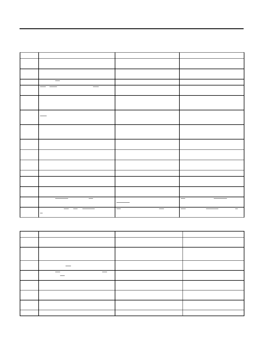
Table 2. 3-Position Jumpers
JUMPER
GENERAL DESCRIPTION
PIN 1-2
PIN 2-3
W1
Connects BP/CH3 (ADC) to R45 or GND;
Input not in use, grounded to reduce noise
Use as single input channel3 or
differential input positive channel B
W2
Connects BM/CH4 (ADC) to R44 or GND;
Input not in use, grounded to reduce noise
Use as single input channel4 or
differential input negative channel B
W3
Connects RD to XF or /RD1
Logic generator is connected to the ADC
DSP is connected to the ADC
W4
WR + WR1 is connected with DSP_WR or
U12-J9/3
Logic generator is connected to the ADC
DSP is connected to the ADC
W5
W6
W7
The three Jumpers define the prescaling of the
CLKOUT signal to the MCB_CLK Pin, if W8 is
set to Counter-Mode
W8
MCB_CLK is connected to BUFCLK (U14) or
RD1 (U11)
Counter-Mode (MCB_CLK signal is
divided by the counter, set-up with
Jumper W(5-7)
Counter-Mode disabled (MCB_CLK is
synchronize with the CLKOUT signal)
W9
CLK input of the Counter (U2) is connected with
CLKOUT or CLKOUT/2
The counter is toggled by the DSP
system clock (signal BUFF_CLK)
The counter’s clock is prescaled by two
(toggled by half the DSP system clock
(CLKOUT2))
W10
ADC CLKIN is connected to CLK/2 or CLK/4
The ADC clock runs at a quarter of the
DSP clock frequency (10 MHz)
The ADC clock runs at half the DSP
clock frequency (20 MHz)
W11
Connects AP/CH1 (ADC) to R48 or GND;
Input not in use, grounded to reduce
noise
Use as single input channel 1 or
differential input positive channel A
W12
Connects AM/CH2 (ADC) to R47 or GND;
Input not in use, grounded to reduce
noise
Use as single input channel 2 or
differential input negative channel A
W13
Connects REFLO (TLV5651) to Vcc or GND
Disable internal reference
Enable internal reference
W14
Connects SCLK (TLC5618AA) to BCLKX or J8
(BNC)
Normal DSP mode
An external clock source drives the
SCLK pin instead of the DSP
W15
Connects CLK (TLV5651) to CLKOUT (DSP) or
J7 (BNC)
Normal DSP mode
An external clock source drives the CLK
pin instead of the DSP
W23
Connects CSTART to A0, A1, or XF
A0 and A1 used to generate ADC
CSTART signal
XF signal connects to CSTART pin
W24
Connects DSP_RD to XF or IOSTRB, ORed with
R/W from the DSP
XF signal connected to ADC RD pin
RD pin driven by IOSTRB ORed with R/W
Table 3. 2-Position Jumpers
JUMPER
GENERAL DESCRIPTION
PINS SHORTED
PINS OPEN
W16
Connects Mode input (TLV 5651) to GND
MODE 0 is chosen (binary data input)
MODE 1 is chosen (2s complement
data input)
W17
Connects REFIO (TLV5651) to VREF1 or leaves
the REFIO pin decoupled to GND via a 0.1
µ
F
capacitor
Use as external reference voltage input
Use as internal reference voltage
output with this pin terminated into
GND in series with 0.1 pF
W18
Connects DIR (U19) to GND or leaves the DIR
pin connected to WR
ADC can only write but not read to the data
bus
Normal operation mode
W19
Connects OE (U19) to GND or leaves the OE pin
connected to CS
Output driver is isolated and disabled (no
signal can bus trough the data bus)
Normal operation mode
W20
Connects BDX to BDR or leaves BDR open
DSP BDR pin gets a shortcuted feedback
from the BDX (transmit) pin; normal mode
BDR remains open
W21
Connects BSFX to BSFR or leaves BCLKR open
DSP BSFR pin gets a shortcuted feedback
from the BSFX (transmit) pin; normal mode
BSFR remains open
W22
Connects BCLKX backwards with BCLKR or
leaves it open
DSP BCLKR pin gets a shortcuted feedback
from the BCLKX (transmit) pin; normal mode
BCLKR remains open
W28
Connect Sleep input (TLV5651/5 GND
Normal mode of operation
Sleep mode seleted