5 pcmcia card interface, Features and specifications – Renesas CPU Board M3A-HS19 User Manual
Page 30
Features and Specifications
2.5 PCMCIA Card Interface
Rev.1.01 Oct 28, .2008
2-14
REJ10J1351-0101
2
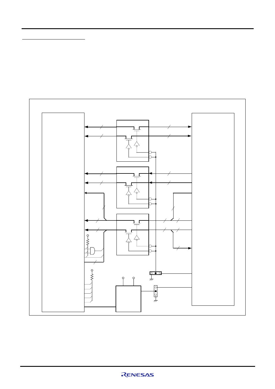
2.5 PCMCIA Card Interface
The SH7619 MCU mounted on the M3A-HS19 is compliant with the JEIDA 4.2 (PCMCIA2.1 Rev.2.1). However, only
3.3 V interface PC card is supported. An on-chip bus state controller (BSC) and a PFC control the PC card.
High byte and low byte of the data is switched at the bus switch on the M3A-HS19. When the byte order of the SH7619 is
big-endian, the order of the PC card connector is little-endian (IOIS16#: ”L”).
The M3A-HS19 is provided with a PCMCIA card slot in area 5, allowing both IC memory card and I/O card to be mounted.
Figure 2.5.1 shows the block diagram of PCMCIA card interface.
PC card connector (J4)
10
PCMCIA
Power supply
circuit
D7-D0, D15, D14
SH7619 (U1)
D13-D8
1A[9:0]
1OE#
2OE#
20-bit bus switch
2A[9:0]
1B[9:0]
2B[9:0]
1A[9:0]
1OE#
2OE#
20-bit bus switch
2A[9:0]
1B[9:0]
2B[9:0]
1A[9:0]
1OE#
2OE#
20-bit bus switch
2A[9:0]
1B[9:0]
2B[9:0]
10
10
10
10
10
6
6
D5-D0
D15-D6
A25-A16
A15-A6
A25-A16
A15-A6
6
4
6
8
10
4
A5-A0
A5-A0
RESET
CE1#
CE2#
REG#
PC09/RX_ER(GPIO)
CE2A#
CE1A#
PC14/COL
OE#
WE#
IORD#
IOWR#
RD#
WE#
PB05/ICIORD#
PB06/ICIOWR#
4
PC15/CRS
PB0/WAIT#
PB1/IOIS16#
PD7/IRQ7
4
4
2
CD1#
CD2#
WAIT#
IOIS16#
IREQ#
3.3 V
x3
JP2
JP1
VS1#
VS2#
INPACK#
SPKR#
STSCHG#
PCVCC
x5
3.3 V
5.0 V
VCC
PC20/WOL
PB13/BS#
PCVCC
Figure 2.5.1 PCMCIA Card Interface