Figure 5.5 timing requirements – Renesas Emulation Pod M306H2T-RPD-E User Manual
Page 62
( 60 / 76 )
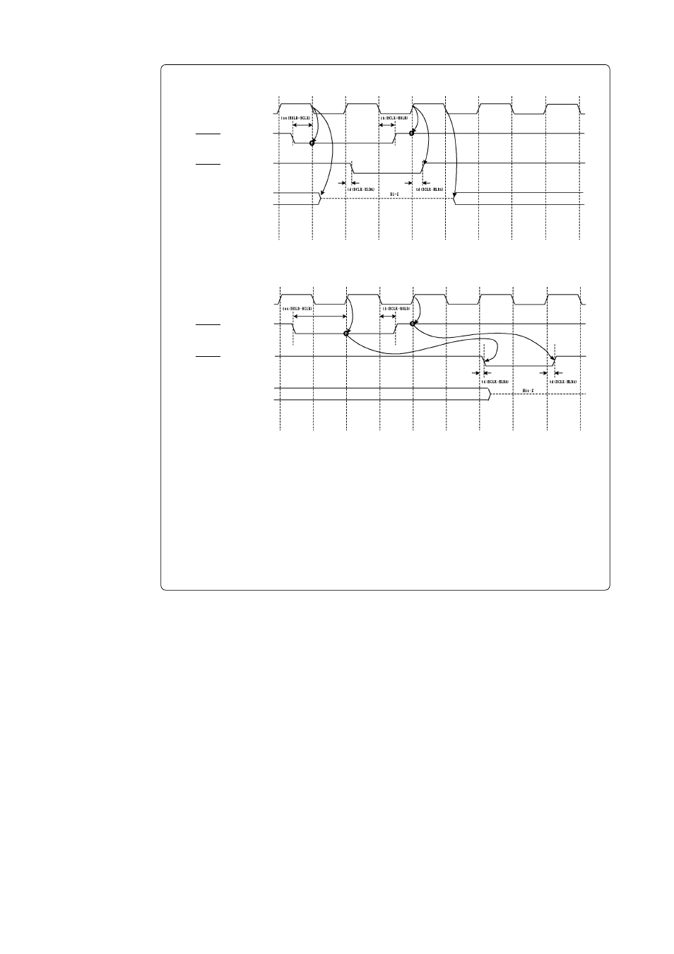
Figure 5.5 Timing requirements
Common to "with wait" and "no-wait" (actual MCU)
BCLK
P0, P1, P2,
P3, P4,
P5
0
to P5
2
Common to "with wait" and "no-wait" (This product)
BCLK
P0, P1, P2,
P3, P4,
P5
0
to P5
2
Note 1. Ports P0
0
to P5
2
will be high-impedance status regardless of the input level of BYTE pin
and ports P4
0
to P4
3
function selection bit (PM06) of the processor mode register 0.
Note 2. This product will be high-impedance status delaying by 2.5 cycles than an actual MCU.
Note 3. The setup time of HOLD is defined by the startup of BCLK, differently from that of actual
MCUs.
Conditions:
• V
CC
= 5 V
• Input timing voltage: V
IL
= 1.0 V, V
IH
= 4.0 V
• Output timing voltage: V
OL
= 2.5 V, V
OH
= 2.5 V
HLDA output
HOLD input
HLDA output
HOLD input
See also other documents in the category Renesas Hardware:
- Single-Chip Microcomputer M34551T2-MCU (42 pages)
- M3T-FLX-80NRA (6 pages)
- 70 (162 pages)
- M16C/30P (102 pages)
- PROM Programming Adapter PCA7427G02 (20 pages)
- R0E572110CFK00 (40 pages)
- H8/325 Series (20 pages)
- Single-Chip Microcomputer H8/36079 (27 pages)
- Direct Dummy IC M3T-DIRECT100S (4 pages)
- M3A-2152 (95 pages)
- PCA7755D (6 pages)
- M16C/6N5 (106 pages)
- SH7085 (50 pages)
- QFP-144 (23 pages)
- H8/3834 Series (22 pages)
- RSKM16C62P (3 pages)
- H8/33937 (22 pages)
- Single-Chip Microcomputer H8SX/1622 (5 pages)
- E6000 (29 pages)
- PCA7400 (18 pages)
- PCA4738FF-64 (20 pages)
- SuperH HS7339KCU01HE (43 pages)
- M16C FAMILY (103 pages)
- PCA7412F-100 (20 pages)
- 4513 (210 pages)
- M34551E8FP (16 pages)
- Dummy IC M3T-SSOP36B-450 (4 pages)
- Emulation Pod M30100T3-RPD-E (52 pages)
- Converter Board for M30102 M30102T-PTC (4 pages)
- SH7145 (31 pages)
- HS1653ECN61H (36 pages)
- Converter Board R0E521276CFG00 (4 pages)
- PCA7302E1F-80 (18 pages)
- H8/3814 Series (21 pages)
- H8S/2646 Series (20 pages)
- SuperHTM Family SH7125 Series (40 pages)
- M30262T-PTC (4 pages)
- SH7670 (82 pages)
- H8/3864 Series (20 pages)
- Emulator System M3T-MR100 (306 pages)
- 38K0 (6 pages)
- PLQP0176KB-A (40 pages)
- Direct Dummy IC M3T-DIRECT80S (6 pages)
- PCA4738L-80A (26 pages)
- Converter Board R0E5212BACFG00 (6 pages)