4) timing requirements – Renesas Emulation Pod M306H2T-RPD-E User Manual
Page 61
( 59 / 76 )
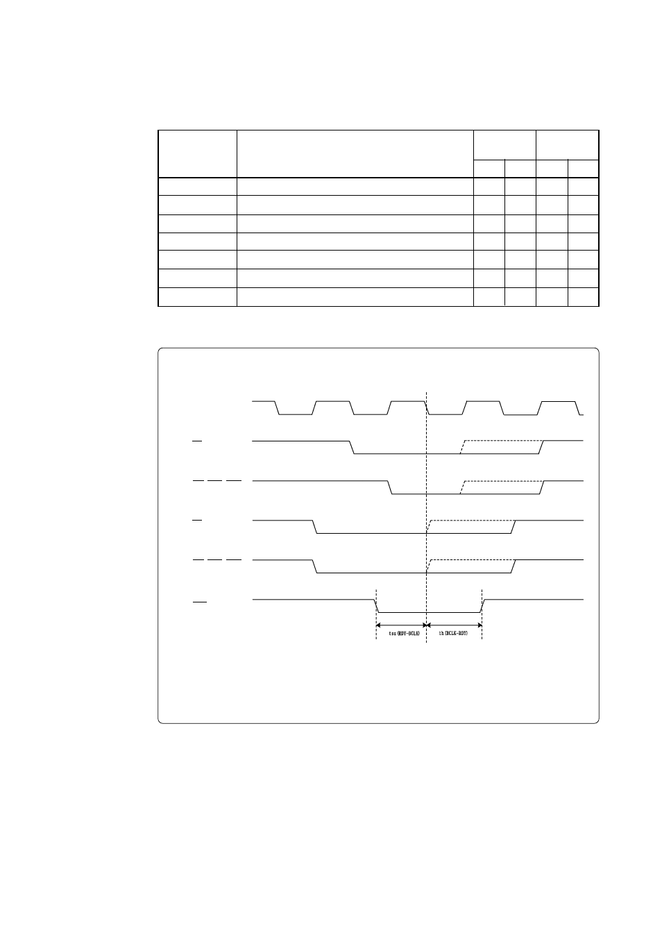
(4) Timing Requirements
Table 5.5, Figures 5.4 and 5.5 show timing requirements in the memory expansion and microprocessor
modes.
Table 5.5 Timing requirements (V
CC
= 5 V)
*1 Minimum 7 ns (The definition is different from that of actual MCUs. For details, see Figure 5.5.)
Figure 5.4 Timing requirements
Memory expansion and microprocessor modes
(only for "with wait")
BCLK
Conditions:
• V
CC
= 5 V
• Input timing voltage: V
IL
= 1.0 V, V
IH
= 4.0 V
• Output timing voltage: V
OL
= 2.5 V, V
OH
= 2.5 V
RDY input
WR, WRL, WRH
(multiplex bus)
RD
(multiplex bus)
WR, WRL, WRH
(separate bus)
RD
(separate bus)
Tsu (DB-RD)
Tsu (RDY-BCLK)
Tsu (HOLD-BCLK)
Th (RD-DB)
Th (BCLK-RDY)
Th (BCLK-HOLD)
Td (BCLK-HLDA)
Data input setup time
RDY* input setup time
HOLD* input setup time
Data input hold time
RDY* input hold time
HOLD* input hold time
HLDA* output delay time
Min.
40
30
40
0
0
0
Max.
40
Min.
45
*1
Max.
Actual MCU
[ns]
This product
[ns]
Symbol
Item
See left
See left
See left
See left
See left
- Single-Chip Microcomputer M34551T2-MCU (42 pages)
- M3T-FLX-80NRA (6 pages)
- 70 (162 pages)
- M16C/30P (102 pages)
- PROM Programming Adapter PCA7427G02 (20 pages)
- R0E572110CFK00 (40 pages)
- H8/325 Series (20 pages)
- Single-Chip Microcomputer H8/36079 (27 pages)
- Direct Dummy IC M3T-DIRECT100S (4 pages)
- M3A-2152 (95 pages)
- PCA7755D (6 pages)
- M16C/6N5 (106 pages)
- SH7085 (50 pages)
- QFP-144 (23 pages)
- H8/3834 Series (22 pages)
- RSKM16C62P (3 pages)
- H8/33937 (22 pages)
- Single-Chip Microcomputer H8SX/1622 (5 pages)
- E6000 (29 pages)
- PCA7400 (18 pages)
- PCA4738FF-64 (20 pages)
- SuperH HS7339KCU01HE (43 pages)
- M16C FAMILY (103 pages)
- PCA7412F-100 (20 pages)
- 4513 (210 pages)
- M34551E8FP (16 pages)
- Dummy IC M3T-SSOP36B-450 (4 pages)
- Emulation Pod M30100T3-RPD-E (52 pages)
- Converter Board for M30102 M30102T-PTC (4 pages)
- SH7145 (31 pages)
- HS1653ECN61H (36 pages)
- Converter Board R0E521276CFG00 (4 pages)
- PCA7302E1F-80 (18 pages)
- H8/3814 Series (21 pages)
- H8S/2646 Series (20 pages)
- SuperHTM Family SH7125 Series (40 pages)
- M30262T-PTC (4 pages)
- SH7670 (82 pages)
- H8/3864 Series (20 pages)
- Emulator System M3T-MR100 (306 pages)
- 38K0 (6 pages)
- PLQP0176KB-A (40 pages)
- Direct Dummy IC M3T-DIRECT80S (6 pages)
- PCA4738L-80A (26 pages)
- Converter Board R0E5212BACFG00 (6 pages)