3 block diagram – Renesas 32185 User Manual
Page 44
32185/32186/32192/32195/32196 Group
Starter Kit User’s Manual M3A-2154G52B
REJ10B0223-0150/Rev.1.50
Mar 2008
Page 36 of 80
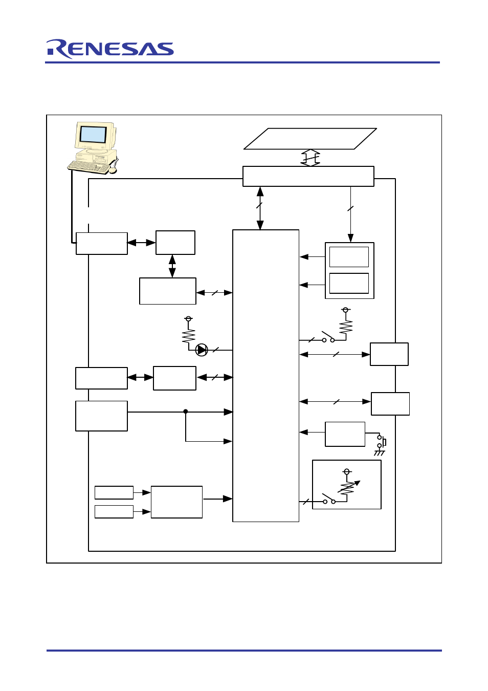
1.3 Block
Diagram
A block diagram of the M3A-2154G02A is shown below.
Figure 1.3 Block Diagram of the M3A-2154G02A
CAN
connector
CAN
driver
SIO
CAN
FP
select
MOD
select
MOD0/
MOD1
FP
VCCE
power supply
connector
VCCE
VCC-BUS
VDDE
VCCER
AVCC
VREF0
Extension connector
Port
JTAG
connector
Reset
circuit
JTAG
RESET
AD
Oscillator
circuit
XIN
RS-232C
cable
Host PC
(Windows)
Extension board
Serial I/O
Channel select
32185/32186/32192/
32195/32196 group MCUs
2
4
8
144
144
5
8
Port13
8
2
(JTAG, MCU control and
other pins excluded)
NBD I/F
connector
NBD I/F
8
(JTAG,MCU control
and other pins excluded)
RS-232C
connector
RS-232C
driver
Port11
10MHz
20MHz
VCC-BUS
/VDDE
/VCCER
/AVCC
/VREF0