Figure 2-15, Configuration register write timing diagram, Figure 2-16 – National Instruments SCXI-1120 User Manual
Page 47: Scxi-1120 module id register timing diagram
Chapter 2
Configuration and Installation
© National Instruments Corporation
2-31
SCXI-1120 User Manual
SLOT0SEL*
SERDATIN
SERCLK
SS*
0
1
0 0 0 0 1 1 0 0 0 0 1 1 1 1
Figure 2-15. Configuration Register Write Timing Diagram
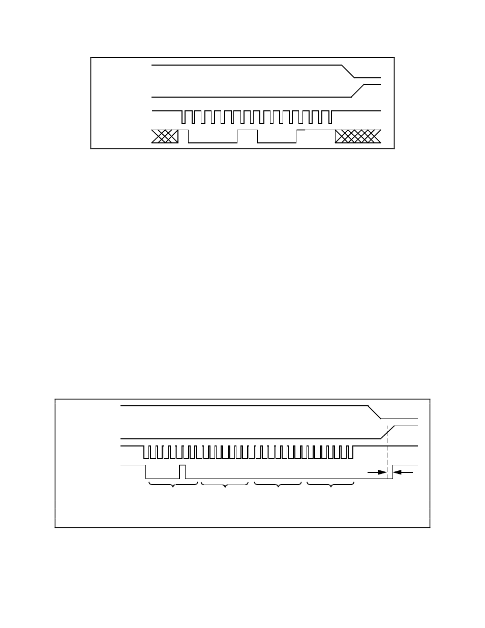
To read from the Module ID Register, follow these steps:
1. Initial conditions:
SS* asserted low.
SERDATIN = don't care.
DAQD*/A = 1. Make sure DAQD*/A does not go low or erroneous data will be written
to the Configuration Register.
SLOT0SEL* = 1.
SERCLK = 1 (and has not changed since SS* went low).
2. For each bit to be read:
SERCLK = 0.
SERCLK = 1. Clock the data.
Read the level of the SERDATOUT line.
3. Pull SLOT0SEL* low to deassert the SS* line and establish conditions for writing a new
slot-select number to the Slot 0 Slot-Select Register.
4. If you are not selecting another slot, you should write zero to the Slot 0 Slot-Select Register.
Figure 2-16 illustrates a read of the SCXI-1120 Module ID Register.
SLOT0SEL*
SS*
SERCLK
0
1
0 0 0 0
0 0 0 0 0 0 0 0 0 0 0 0 0 0 0 0 0 0 0 0 0 0 0 0 0
0
SERDATOUT
T
delay
byte 0 = 4
byte 3 = 0
byte 2 = 0
byte 1 = 0
T
delay
SS* high to SERDATOUT high
350 nsec maximum
Figure 2-16. SCXI-1120 Module ID Register Timing Diagram
For further details on programming these signals, refer to Chapter 5, Programming.