NEC PD78058FY(A) User Manual
Page 407
407
CHAPTER 18 SERIAL INTERFACE CHANNEL 1
Data Transfer Interval Specification (f
XX
= 5.0 MHz Operation)
ADTI4 ADTI3 ADTI2 ADTI1
1
1
1
1
1
1
1
1
1
1
1
1
1
1
1
1
0
0
0
0
0
0
0
0
1
1
1
1
1
1
1
1
0
0
0
0
1
1
1
1
0
0
0
0
1
1
1
1
0
0
1
1
0
0
1
1
0
0
1
1
0
0
1
1
Minimum
Note
223.2
s + 0.5/f
SCK
236.0
s + 0.5/f
SCK
248.8
s + 0.5/f
SCK
261.6
s + 0.5/f
SCK
274.4
s + 0.5/f
SCK
287.2
s + 0.5/f
SCK
300.0
s + 0.5/f
SCK
312.8
s + 0.5/f
SCK
325.6
s + 0.5/f
SCK
338.4
s + 0.5/f
SCK
351.2
s + 0.5/f
SCK
364.0
s + 0.5/f
SCK
376.8
s + 0.5/f
SCK
389.6
s + 0.5/f
SCK
402.4
s + 0.5/f
SCK
415.2
s + 0.5/f
SCK
Maximum
Note
224.8
s + 1.5/f
SCK
237.6
s + 1.5/f
SCK
250.4
s + 1.5/f
SCK
263.2
s + 1.5/f
SCK
276.0
s + 1.5/f
SCK
288.8
s + 1.5/f
SCK
301.6
s + 1.5/f
SCK
314.4
s + 1.5/f
SCK
327.2
s + 1.5/f
SCK
340.0
s + 1.5/f
SCK
352.8
s + 1.5/f
SCK
365.6
s + 1.5/f
SCK
378.4
s + 1.5/f
SCK
391.2
s + 1.5/f
SCK
404.0
s + 1.5/f
SCK
416.8
s + 1.5/f
SCK
6
5
4
3
2
1
0
7
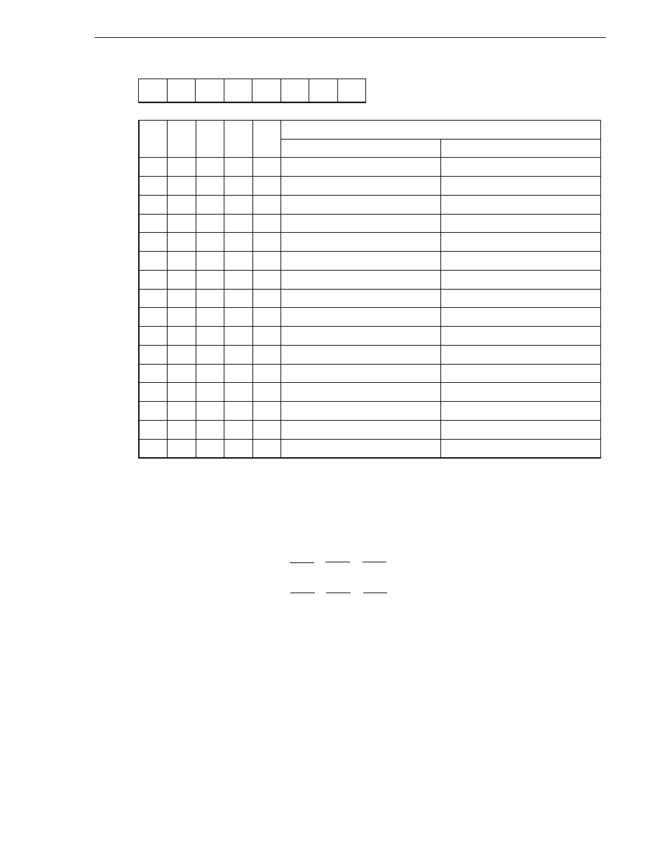
Symbol
ADTI ADTI7
0
0
ADTI4 ADTI3 ADTI2 ADTI1 ADTI0
FF6BH 00H R/W
Address After Reset R/W
ADTI0
0
1
0
1
0
1
0
1
0
1
0
1
0
1
0
1
µ
µ
µ
µ
µ
µ
µ
µ
µ
µ
µ
µ
µ
µ
µ
µ
µ
µ
µ
µ
µ
µ
µ
µ
µ
µ
µ
µ
µ
µ
µ
µ
Note
The data transfer interval includes an error. The data transfer minimum and maximum intervals
are found from the following expressions (n: Value set in ADTI0 to ADTI4). However, if a minimum
which is calculated by the following expressions is smaller than 2/f
SCK
, the minimum interval time
is 2/f
SCK
.
Minimum = (n+1)
×
+
+
Maximum = (n+1)
×
+
+
Cautions 1. Do not write ADTI during operation of automatic data transmit/receive function.
2. Bits 5 and 6 must be set to zero.
3. If the auto send and receive data transmission interval time is controlled using ADTI,
busy control becomes invalid (see 18.4.3 (4) (a) Busy control option).
Remarks 1. f
XX
:
Main system clock frequency (f
X
or f
X
/2)
2. f
X
:
Main system clock oscillation frequency
3. f
SCK
:
Serial clock frequency
2
6
f
XX
2
6
f
XX
28
0.5
f
XX
f
SCK
36
1.5
f
XX
f
SCK