2 clock output control circuit configuration, 3 clock output function control registers – NEC PD78058FY(A) User Manual
Page 254

254
CHAPTER 12 CLOCK OUTPUT CONTROL CIRCUIT
12.2 Clock Output Control Circuit Configuration
The clock output control circuit consists of the following hardware.
Table 12-1. Clock Output Control Circuit Configuration
Item
Configuration
Timer clock select register 0 (TCL0)
Port mode register 3 (PM3)
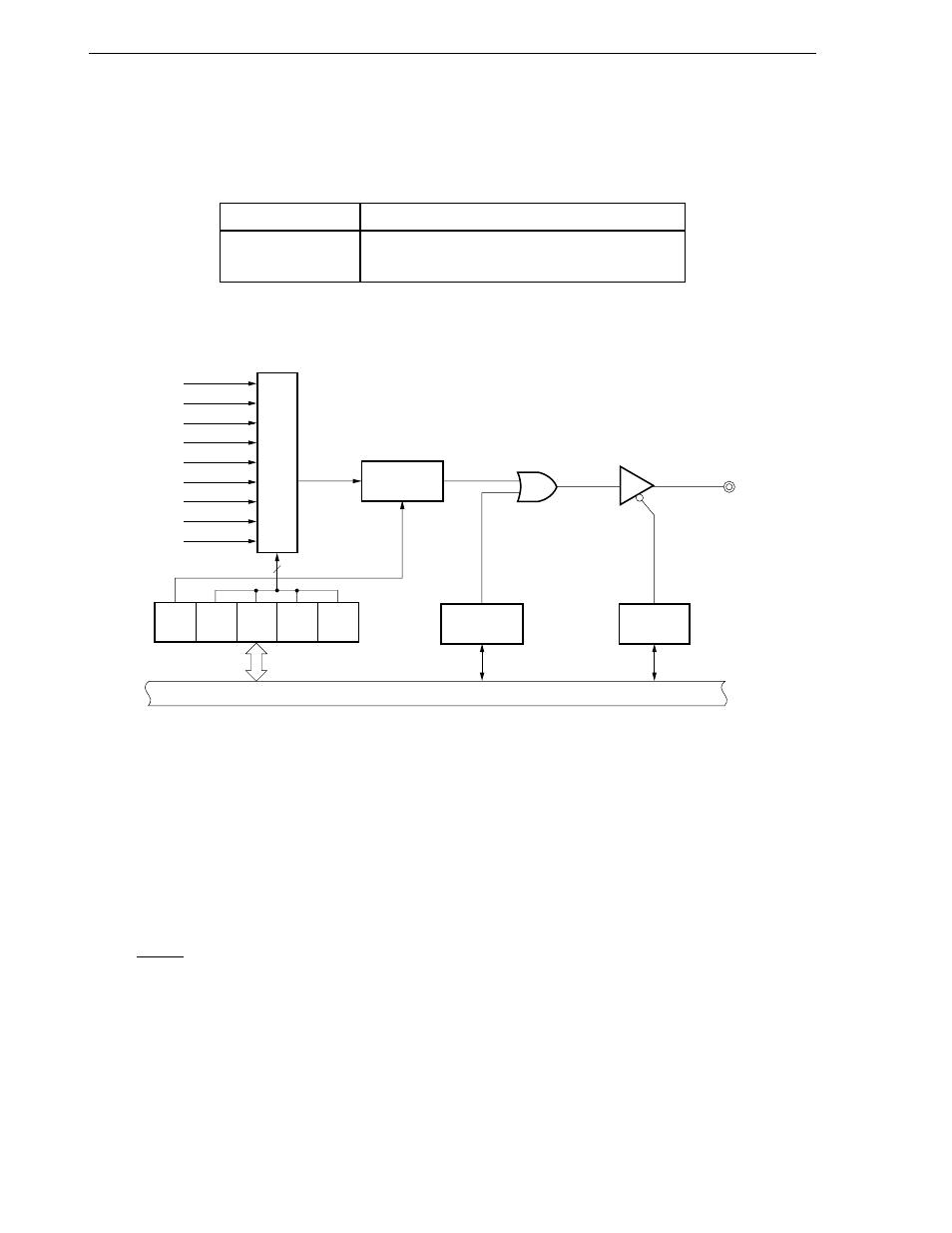
Figure 12-2. Clock Output Control Circuit Block Diagram
12.3 Clock Output Function Control Registers
The following two types of registers are used to control the clock output function.
• Timer clock select register 0 (TCL0)
• Port mode register 3 (PM3)
(1) Timer clock select register 0 (TCL0)
This register sets PCL output clock.
TCL0 is set with a 1-bit or 8-bit memory manipulation instruction.
RESET input sets TCL0 to 00H.
Remark
Besides setting PCL output clock, TCL0 sets the 16-bit timer register count clock.
Control register
Internal Bus
f
XX
f
XX
/2
f
XX
/2
2
f
XX
/2
3
f
XX
/2
4
f
XX
/2
5
f
XX
/2
6
f
XX
/2
7
f
XT
CLOE TCL03 TCL02 TCL01 TCL00
P35
Output Latch
Synchronizing
Circuit
4
PM35
Selector
Timer Clock Select Register 0
Port Mode Register 3
PCL /P35
