Figure 2-6. serial data timing diagram, Figure 2-6, Serial data timing diagram – National Instruments SCXI-1163 User Manual
Page 35
Configuration and Installation
Chapter 2
SCXI-1163 User Manual
2-20
© National Instruments Corporation
To write the 16-bit slot-select number to Slot 0, follow these steps:
1. Initial conditions:
SERDATIN = don't care.
DAQD*/A = 1.
SLOT0SEL* = 1.
SERCLK = 1.
2. Clear SLOT0SEL* to 0. This deasserts all SS* lines to all modules in all chassis.
3. For each bit, starting with the MSB, perform the following action:
a. SERDATIN = bit to be sent. These bits are the data that are being written to the
Slot-Select Register.
b. SERCLK = 0.
c. SERCLK = 1. This rising edge clocks the data.
4. Set to 1. This asserts the SS* line of the module whose slot number was written to Slot 0. If
you are using multiple chassis, only the appropriate slot in the chassis whose address
corresponds to the written chassis number is selected. When no communication is taking
place between the data acquisition board and any modules, write zero to the Slot-Select
Register to ensure that no accidental writes occur.
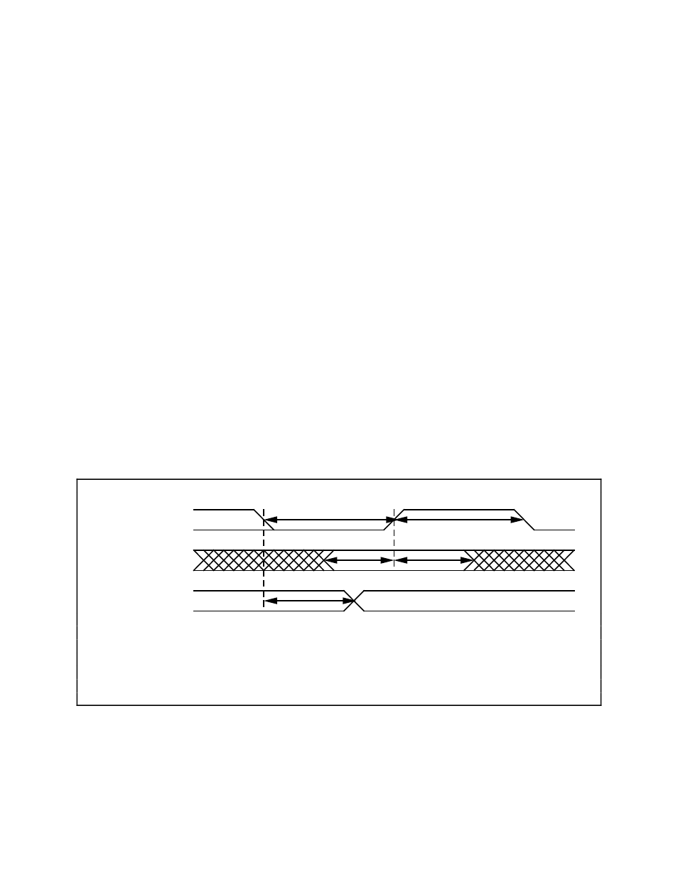
Figure 2-6 shows the timing requirements on the SERCLK and SERDATIN signals. You must
observe these timing requirements for all communications. T
delay
is a specification of the
SCXI-1163.
T
low
T
high
SERCLK
SERDATIN
SERDATOUT
T
setup
T
hold
T
delay
T
low
Minimum low time
65 nsec minimum
T
high
Minimum high time
400 nsec minimum
T
setup
SERDATIN setup time
200 nsec minimum
T
hold
SERDATIN hold time
200 nsec minimum
T
delay
SERDATOUT delay
350 nsec maximum
Figure 2-6. Serial Data Timing Diagram
After you select the module slot as previously described, each write or read cycle to the module
requires you to write first to the Address Handler, then to the register of interest.