Table 2-3 – National Instruments SCXI-1163 User Manual
Page 33
Configuration and Installation
Chapter 2
SCXI-1163 User Manual
2-18
© National Instruments Corporation
When you configure the SCXI-1163 for an MIO-type board, the digital I/O signals of the
SCXI-1163 match the digital I/O lines of the MIO board. When you use the SCXI-1163 with an
SCXI-1341, SCXI-1342, or SCXI-1344 cable assembly, the SCXI-1163 signals match the digital
lines of the Lab-NB/Lab-PC/Lab-PC+ boards, the PC-LPM-16 board, and the Lab-LC board,
respectively. When you configure the SCXI-1163 for a DIO-type board, the digital I/O signals
of the SCXI-1163 match the digital I/O lines of the DIO-24 and DIO-96. When used with an
SCXI-1348 cable assembly, the SCXI-1163 signals match the digital lines of the DIO-32F.
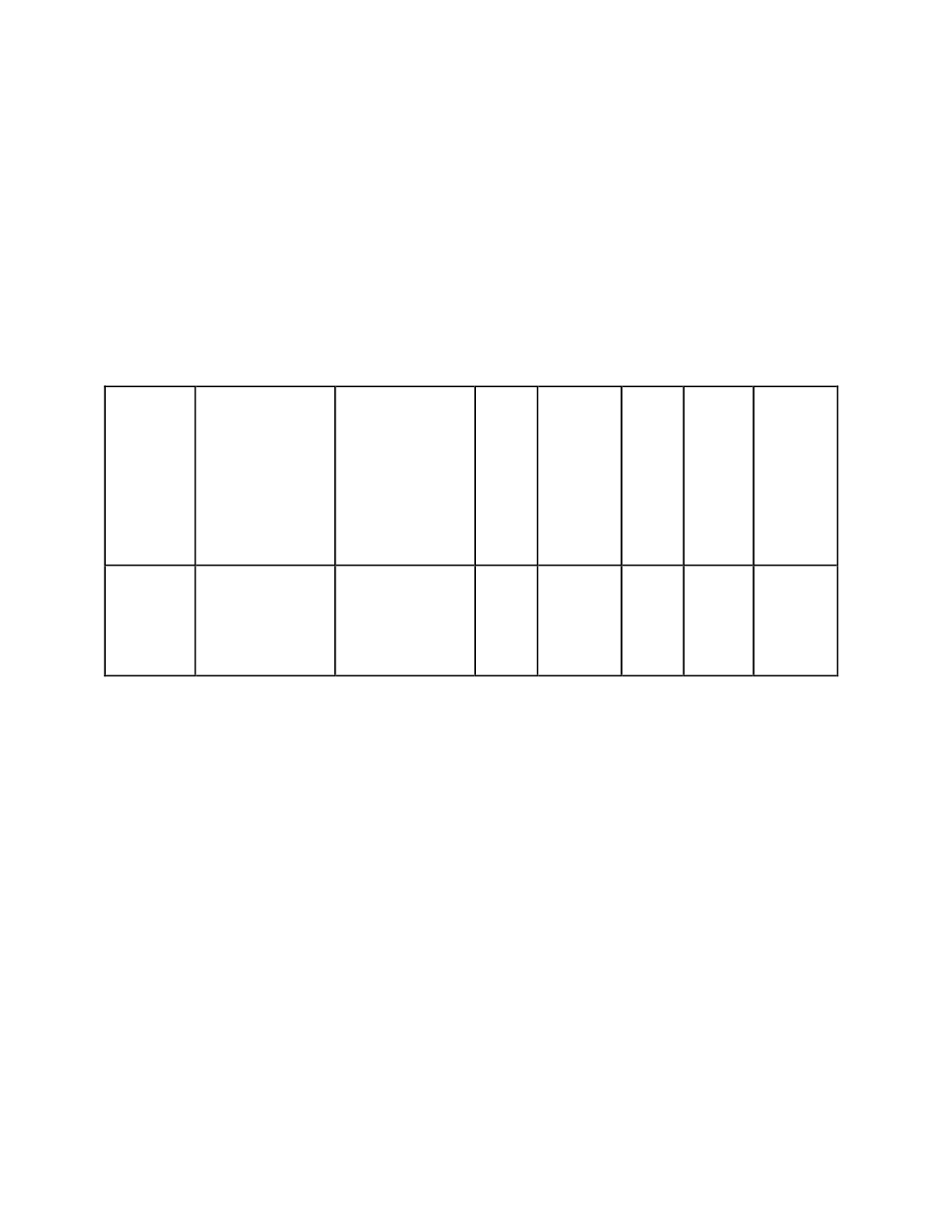
Table 2-3 lists the pin equivalences. For more information, consult Appendix E,
Table 2-3. SCXIbus to SCXI-1163 Rear Signal Connector to Data Acquisition Board
Pin Equivalences
SCXIbus Line
SCXI-1163 Rear
Signal Connector
MIO Boards
Lab-NB/Lab-PC/
Lab-PC+/Lab-LC
PC-LPM-16
DIO-24
DIO-96
DIO-32F
MOSI
D*/A
INTR*
SPICLK
MISO
SERDATIN
DAQD*/A
SLOT0SEL*
SERCLK
SERDATOUT
ADIO0
ADIO1
ADIO2
EXTSTROBE*
BDIO0
PB4
PB5
PB6
PB7
PC1
DOUT4
DOUT5
DOUT6
DOUT7
DIN6
PB3
PB2
PB1
PB0
PA0
APB3
APB2
APB1
APB0
APA0
DIOB3
DIOB2
DIOB1
DIOB0
DIOA0
The following specifications and ratings apply to the digital I/O lines.
Absolute maximum voltage
input rating
5.5 V with respect to DIG GND
Digital input specifications (referenced to DIG GND):
V
IH
input logic high voltage
2 V minimum
V
IL
input logic low voltage
0.8 V maximum
I
I
input current leakage
±
1
µ
A maximum
Digital output specifications (referenced to DIG GND):
V
OH
output logic high voltage
3.7 V minimum at 4 mA maximum
V
OL
output logic low voltage
0.4 V maximum at 4 mA maximum