Timing requirements and communication protocol, Communication signals, Figure 2-5. slot-select timing diagram – National Instruments SCXI-1163 User Manual
Page 34: Figure 2-5, Slot-select timing diagram, See the, Section later in this chapter, and
Chapter 2
Configuration and Installation
© National Instruments Corporation
2-19
SCXI-1163 User Manual
Timing Requirements and Communication Protocol
Communication Signals
This section describes the methods for communicating on the Serial Peripheral Interface (SPI)
bus and their timing requirements. The communication signals are SERDATIN, DAQD*/A,
SLOT0SEL*, SERDATOUT, and SERCLK. Because SS* is produced by Slot 0 according to
data acquisition board programming, this section also discusses SS* timing relationships. For
information on the Slot 0 Slot-Select Register, consult Chapter 4,
The data acquisition board writes a slot-select number to Slot 0 to determine to which slot it will
talk. In the case of an SCXI-1001 chassis, this write also determines to which chassis the data
acquisition board will talk.
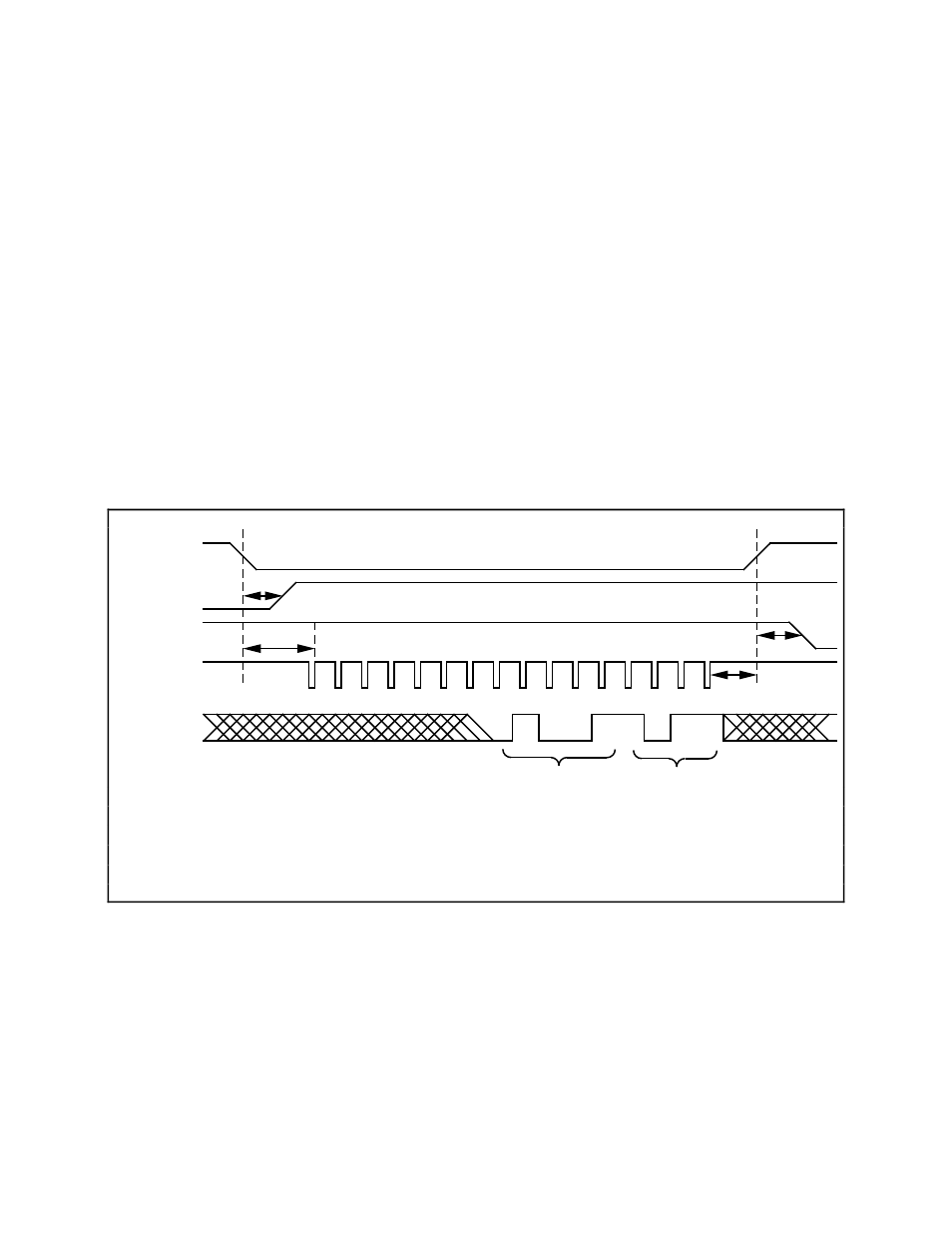
Use the following procedure for selecting a slot in a particular chassis. Figure 2-5 shows the
timing of this procedure with the example of selecting Slot 11 in Chassis 9. Notice that the
factory-default chassis address for the SCXI-1000 is address 0. For information on changing the
address of your chassis, consult the SCXI-1000/1001 User Manual. An SCXI-1000 chassis will
respond to any chassis number.
0
1
0
0
1
1
0
1
1
Chassis ID = 9
Slot 11
SERDATIN
SS*X
Chassis Y
SS*11
Chassis 9
SERCLK
SLOT0SEL*
T
ss_dis
T
ss_en
T
clk_wait
T
slot0sel*_wait
T
ss _ dis
SLOT0SEL* low to SS* disabled
200 nsec maximum
T
clk _ wait
SLOT0SEL* low to first rising edge on SERCLK
75 nsec minimum
T
slot0sel* _ wait
Last rising edge on SERCLK to SLOT0SEL* high
250 nsec minimum
T
ss _ en
SLOT0SEL* high to SS* enabled
350 nsec maximum
Figure 2-5. Slot-Select Timing Diagram