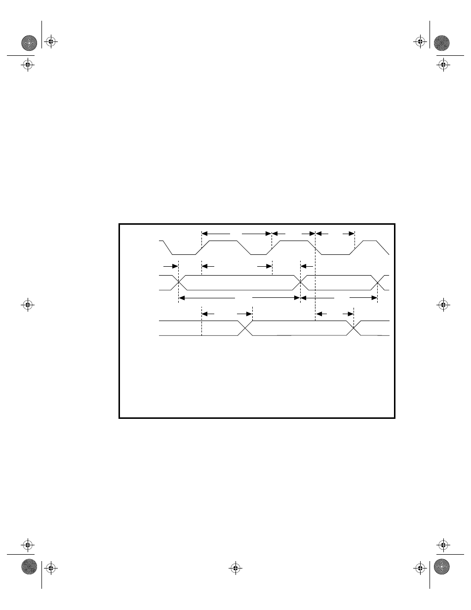
Figure 4-7. general-purpose timing signals, Figure 4-7, General-purpose timing signals -12 – National Instruments PC-LPM-16/PnP User Manual
Page 42
Chapter 4 Signal Connections
PC-LPM-16/PnP User Manual
4-12
National Instruments Corporation
MSM82C53 digital input specifications (referenced to DGND):
•
V
IH
input logic high voltage
2.2 V min
•
V
IL
input logic low voltage
0.8 V max
•
Input load current
±
10.0
µ
A max
MSM82C53 digital output specifications (referenced to DGND):
•
V
OH
output logic high voltage
3.7 V min
•
V
OL
output logic low voltage
0.45 V max
•
I
OH
output source current, at V
OH
1.0 mA max
•
I
OL
output sink current, at V
OL
4.0 mA max
Figure 4-7.
General-Purpose Timing Signals
The GATE and OUT signals in Figure 4-7 are referenced to the rising
edge of the CLK signal.
toutc
tgwl
tgwh
tsc
V
IH
V
IL
V
IH
V
IL
V
OH
V
OL
tpwh
tpwl
tgh
tgsu
toutg
tsc
clock period
125 ns min
tpwh
clock high level
60 ns min
tpwl
clock lowlevel
60 ns min
tgsu
gate setup time
60 ns min
tgh
gate hold time
60 ns min
tgwh
gate high level
60 ns min
tgwl
gate low level
60 ns min
toutg
output delay from clock
60 ns min
toutc
output delay from gate
60 ns min
CLK
GATE
OUT
a.Book : h.chapter 4 Page 12 Wednesday, November 20, 1996 6:36 PM