9 summary, Sd chip – IBM 990 User Manual
Page 49
Chapter 2. System structure and design
37
SD chip
The level 2 cache (L2) is implemented on the four System Data (SD) cache chips, each with a
capacity of 8 MB, providing a cache size of 32 MB. These chips measure 17.5 x 17.5 mm and
carry 521 million transistors, making them the world’s densest chips.
The
dual-core PU chips share the path to the SC chip (L2 control) and the clock chip (CLK).
2.1.9 Summary
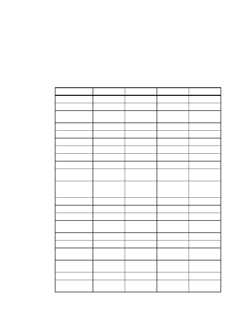
Table 2-2 summarizes all aspects of the z990 system structure.
Table 2-2 System structure summary
IBM 2084-A08
IBM 2084-B16
IBM 2084-C24
IBM 2084-D32
Number of MCMs
1
2
3
4
Total number of PUs
12
24
36
48
Maximum number of
characterized PUs
8
16
24
32
Number of CPs
0 - 8
0 - 16
0 - 24
0 - 32
Number of IFLs
0 - 8
0 - 16
0 - 24
0 - 32
Number of ICFs
0 - 8
0 - 16
0 - 16
0 - 16
Number of zAAPs
0 - 4
0 - 8
0 - 12
0- 16
Standard SAPs
2
4
6
8
Standard spare PUs
2
4
6
8
Number of memory
cards
2
4
6
8
Enabled Memory
Sizes (multiples of 8
GB)
16 - 64 GB
16 - 128 GB
16 - 192 GB
16 - 256 GB
L1 Cache per PU
256/256 KB
256/256 KB
256/256 KB
256/256 KB
L2 Cache
32 MB
64 MB
96 MB
128 MB
Cycle time (ns)
0.83
0.83
0.83
0.83
Maximum number of
STIs
12
24
36
48
STI bandwidth/STI
2.0 GBps
2.0 GBps
2.0 GBps
2.0 GBps
Max STI bandwidth
24 GBps
48 GBps
72 GBps
96 GBps
Maximum number of
I/O cages
3
3
3
3
Number of Support
Elements
2
2
2
2
External power
3 phase
3 phase
3 phase
3 phase
Internal Battery
Feature
optional
optional
optional
optional