Absolute maximum ratings, Dc characteristics (t, 0°c to +70°c; v – Maxim Integrated DS5001FP User Manual
Page 11: 5v ±10%)
DS5001FP
11 of 26
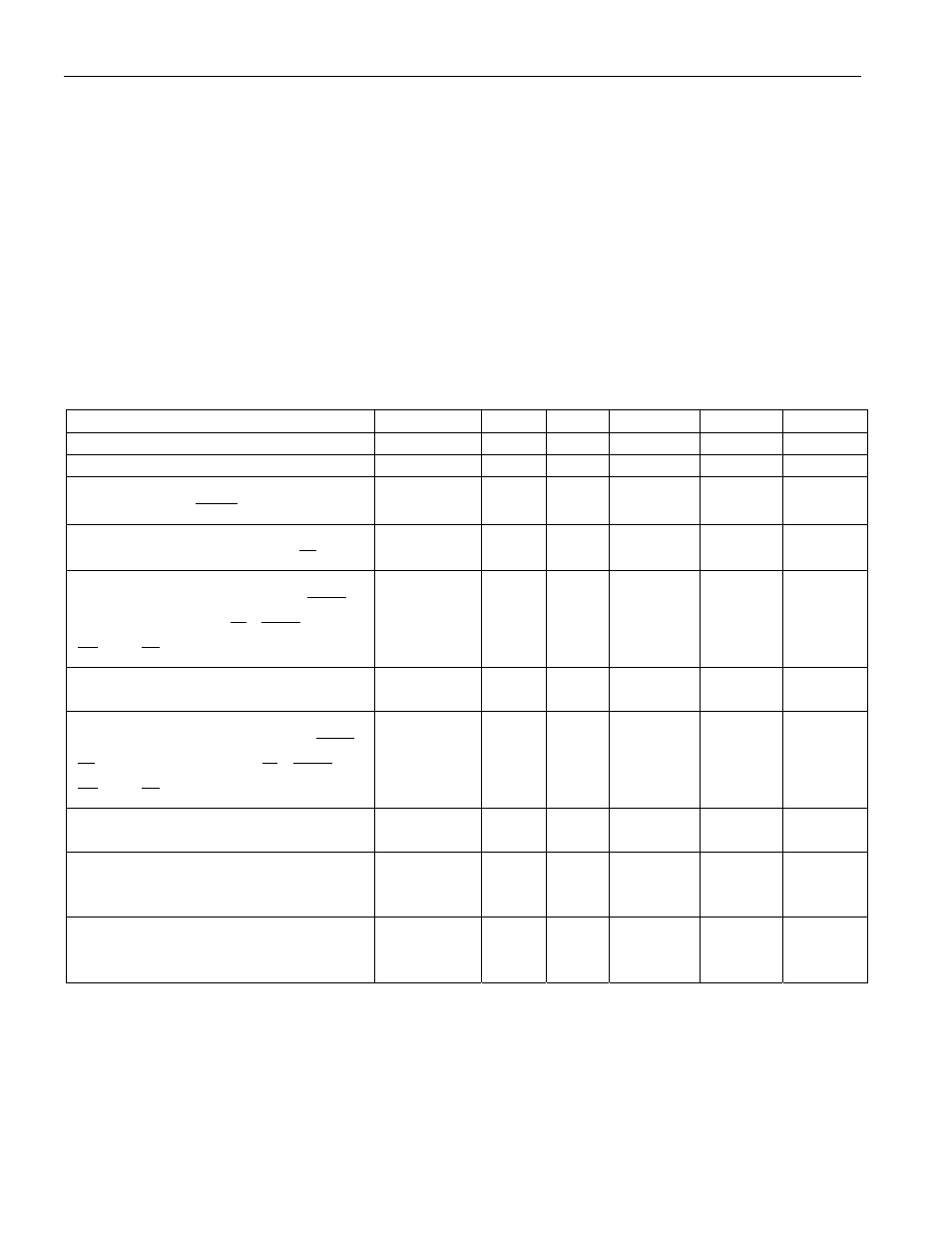
ABSOLUTE MAXIMUM RATINGS*
Voltage Range on Any Pin Relative to Ground
-0.3V to (V
CC
+ 0.5V)
Voltage Range on V
CC
Related to Ground
-0.3
°C to 6.0°C
Operating Temperature Range
-40
°C to +85°C
Storage Temperature Range
1
-55
°C to +125°C
Soldering Temperature
See IPC/JEDEC J-STD-020A
*
This is a stress rating only and functional operation of the device at these or any other conditions above
those indicated in the operation sections of this specification is not implied. Exposure to absolute
maximum rating conditions for extended periods of time may affect reliability.
1
Storage temperature is defined as the temperature of the device when V
CC
= 0V and V
LI
= 0V. In this
state, the contents of SRAM are not battery-backed and are undefined.
DC CHARACTERISTICS (T
A
= 0°C to +70°C; V
CC
= 5V ±10%)
PARAMETER
SYMBOL
MIN
TYP
MAX
UNITS
NOTES
Input Low Voltage
V
IL
-0.3
+0.8
V
1
Input High Voltage
V
IH1
2.0
V
CC
+ 0.3
V
1
Input High Voltage
(RST, XTAL1,
PROG
)
V
IH2
3.5
V
CC
+ 0.3
V
1
Output Low Voltage
at I
OL
= 1.6mA (Ports 1, 2, 3,
PF
)
V
OL1
0.15
0.45
V
1, 11
Output Low Voltage
at I
OL
= 3.2mA (Ports 0, ALE,
PSEN
,
BA15–0, BD7–0, R/
W
,
CE1N
,
CE
1–4,
PE
1–4, V
RST
)
V
OL2
0.15
0.45
V
1
Output High Voltage
at I
OH
= -80µA (Ports 1, 2, 3)
V
OH1
2.4
4.8
V
1
Output High Voltage
at I
OH
= -400µA (Ports 0, ALE,
PSEN
,
PF ,
BA15–0, BD7–0, R/
W
,
CE1N
,
CE
1–4,
PE
1–4, V
RST
)
V
OH2
2.4
4.8
V
1
Input Low Current
V
IN
= 0.45V (Ports 1, 2, 3)
I
IL
-50
µA
Transition Current; 1 to 0
V
IN
= 2.0V (Ports 1, 2, 3)
(0°C to +70°C)
I
TL
-500
µA
Transition Current; 1 to 0
V
IN
= 2.0V (Ports 1, 2, 3)
(-40°C to +85°C)
I
TL
-600
µA
10