Pex8605, 4 clocks 2.4.1 clock source and line termination, 2 clock input pins – Avago Technologies PEX 8605 User Manual
Page 4: 5 reset, 6 configuration straps
PEX8605
© PLX Technology, www.plxtech.com
Page 4 of 13
2 May 2013, version 1.7
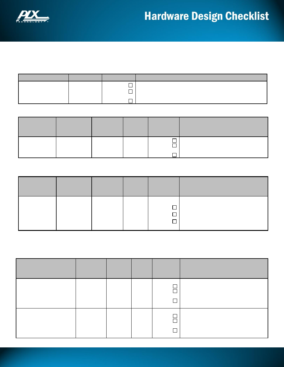
2.4 Clocks
2.4.1 Clock Source and Line Termination
REFCLK Source
Signal Type
Checked
Requirements
External REFCLK Clock
Transmitter
External-CML
YES
NO
UNKNOWN
Frequency Tolerance: ± 300 ppm, max.
33 Ω series (in-line) and 49 Ω shunt (to GND) required on each differential
signal, near the clock source.
2.4.2 Clock Input Pins
Signal Name
Dual-Row
QFN Pkg.
Pin #
TQFP
Package
Pin #
Signal
Type
Checked
Recommendations
PEX_REFCLKn ,
PEX_REFCLKp
B24
A27
52
51
CML Input
YES
NO
UNKNOWN
100 MHz PCI Express Reference Clock input
pair.
2.5 Reset
Signal Name
Dual-Row
QFN Pkg.
Pin #
TQFP
Package
Pin #
Signal
Type
Checked
Recommendations
PEX_PERST#
B15
32
I
YES
NO
UNKNOWN
PCI Express Reset
Used to initiate a fundamental reset. This reset is
propagated to all downstream ports. Adapter card
designs connect this pin directly to the PCI
Express slot PERST# pin. PEX_PERST# should
remain asserted for 100 ms after power supplies
and clocks are stable.
2.6 Configuration Straps
These pins should be pulled High (to VDD_IO) or Low (to Ground), through 4.7K-10K ohms, as indicated.
Signal Name
Dual-Row
QFN Pkg.
Pin #
TQFP
Package
Pin #
Signal
Type
Checked
Recommendations
STRAP_DEBUG_SEL#
C4
30
I
PU
YES
NO
UNKNOWN
Factory Test Only
This signal can be left unconnected in normal
applications. If this ball is connected to a board
circuit trace, it must be externally pulled up to
VDD_IO.
STRAP_FAST_BRINGUP#
A40
78
I
PU
YES
NO
UNKNOWN
Factory Test Only
This signal can be left unconnected in normal
applications. If this ball is connected to a board
circuit trace, it must be externally pulled up to
VDD_IO.