Introduction, Timer 0, J3 connector pin out – Remote Processing RPC-220 User Manual
Page 30
COUNTER/TIMERS
SECTION 8
Page 8-1
J3
Pin
N a m e
Timing
function
1
P 1. 0
CTOI
2
P 4. 3
CMSR3
3
P 1. 1
CT1I
4
RTC
Square wave
5
P 1. 2
CT2I
6
P 3. 2
T0 gate
7
P 1. 3
CT3I
8
+ 5V
9
P 1. 4
T2 clock
10
Reset
11
P 1. 5
T2 reset
12
Ground
13
P 4. 5
CMSR5
14
Ground
15
P 1. 6
16
P 4. 4
CMSR4
17
P 1. 7
18
+ 5V
19
P 3. 4
T0 clock
20
P W M 1
21
P 3. 5
T1 clock
22
P W M 0
23
P 3. 3
T1 gate
24
P 4. 6
CMT0
25
RTC IRQ
26
P 4. 7
CMT1
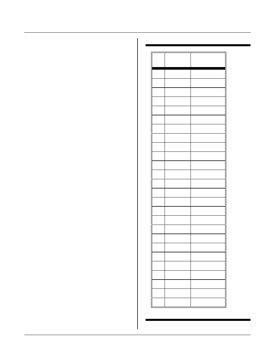
Table 8-1 J3 timing pins
INTRODUCTION
COUNTE R/TIMERS
S E C T IO N 8
The 80C552 C PU chip on the RPC -220 has many
counter/timer s. These ar e used to count pulses or
measur e pulse width s. So me of thes e timer s are m ulti-
purpose , an d are sha red w ith other fun ctions. Timer 1 is
used as the baud rate generator for COM 0. Some lines
used for timing are also used for other functions, such as
LCD display and softw are ser ial port.
The optional RTC can gener ate periodic interrupts on
INT1. See SECTION 7, INTERRUPTS for more
information.
Timer operation is described in detail in two PDF files.
FAM HDW R.P DF descr ibes timers 0 and 1 and
8XC552OV .P DF descr ibes timer 2. Review the
application programs listed at the end of this section.
T i m er s 0 a n d 1 o pe r a te th e sa m e as o n t he 8 0C 5 1 C P U .
TIMER 0
Timers 0 and 1 ar e very similar to each other. Since the
serial port is used for most applications, timer 1 is not
described.
Timer 0 uses an external or internal clock. When
operating on an external clock, it is effectively a counter.
Pulses go into port P3.4, available at J3-19. Pulses are
gated by the T CON and TM OD r egisters an d INT 0 pin
on J3-6 and J2-6. These pins have "soft" pull ups and
may require exter nal resistors to operate reliably.
Maximum clock frequency to timer 0 is 921.6 Khz and
the minimum pulse width is 542 nano-seconds. The
timers operate in one of 4 modes and generate an
interrupt on a terminal count. Refer to the
FAM HDW R.P DF file for a com plete description of
these modes.
J3 CONNECTOR PIN OUT
The table below is the pin out for J3 and associated
timing and alternate func tions.