Block diagram, Chapter 2, System components – Lanner LEC-2110 User Manual
Page 7: Ich8-m, Pineview
7
System Components
Chapter 2
Embedded and Industrial Computing
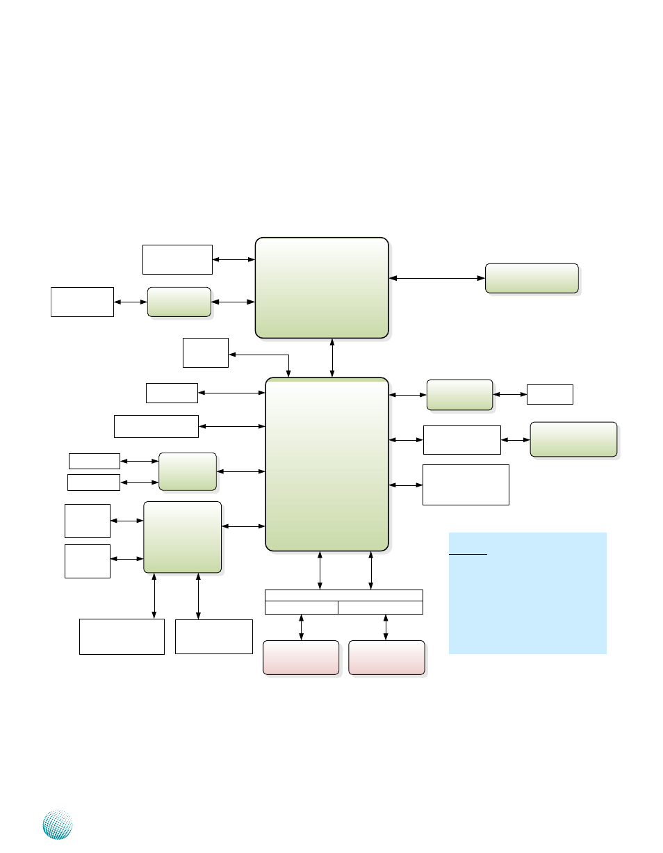
Block Diagram
The block diagram depicts the relationships among the
interfaces and modules on the motherboard..
ICH8-M
mBGA
PINEVIEW
ATOM D525
(FCBGA8)
DDR3
1x SO-DIMM up to 4GB
Fintek
F81865F
SATA Port 0
USB
SPI
Mini PCIexpress
Socket
GbE LAN
Realtek
RTL81111E
2x PCIe
2x RJ-45
USB 2.0
6x Port-A (front I/O)
1x Pin Header
SATA Connector
6 Gbps
PCIe
USB 2.0
VGA
Up to 2048x1536
DVI-D
Up to 1920x1080
DVI
SPI ROM
SST 16M
3G Card +
SIM Card Reader
Serial
PCIe
MIC IN
HD Audio
Codec
ALC 888S
Voltage
Thermal
Sensor
Transmitter
CH7036
LVDS
1366 X 768 MAX.
CF Socket
with WOL/PXE
DMI x 4
LPC
Line Out
COM 2/3
RS-232/422/485
with auto-flow Control
LEK-P01*
1X PCI
LEK-E01*
1X PCIexpress 1X
PCI
Gold finger
PCIexpress 1X
PCI
PCI
PCIe
COM 1/4/5/6
RS-232
Serial
Remark*
The expansion gold finger is flexible
for PCI and PCIe 1X signals;
For LEC-2110, the daughter board
LEK-PO1 or LEK-E01 are selected by
different SKUs.
*LEK- P01 is for LEC-2110P
* LEK-E01 is for LEC-2110E
PS/2
KB/MS
Pin header
Intel Inte
grated
GMA 315
0