Connectors and jumpers list, Chapter 3, Board layout – Lanner LEC-2110 User Manual
Page 12
12
Board Layout
Chapter 3
Embedded and Industrial Computing
Connectors and Jumpers List
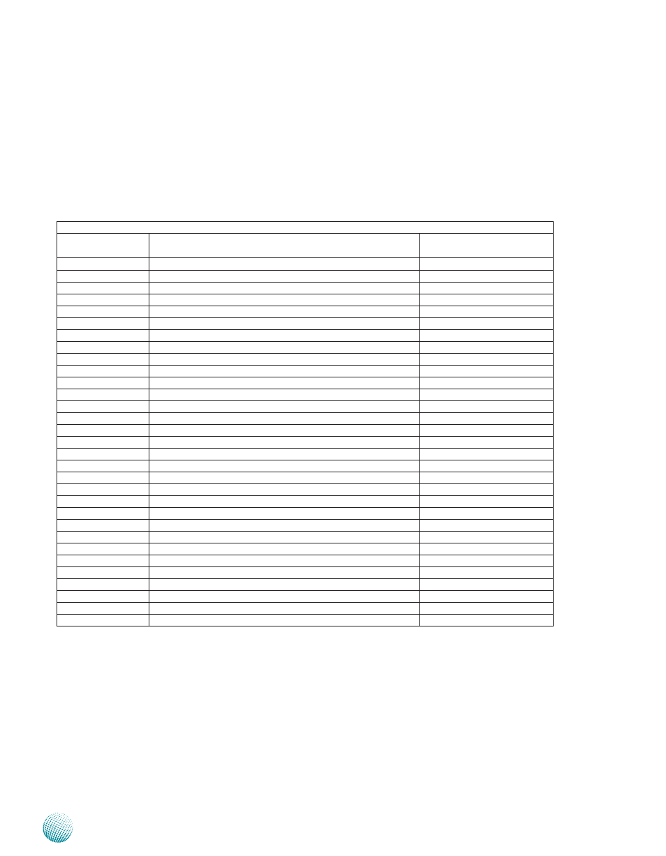
The tables below list the function of each of the board
jumpers and connectors by labels shown in the above
section. The next section in this chapter gives pin
definitions and instructions on setting jumpers.
Table 3.1 Connector List for LEB-2110A
Labels
Function
Pin Definition Reference
Page
CF1
CompactFlash Connector
P17
CMOS1
Clear CMOS Jumper
P14
CN1
DC-in Connector
P17
CN2
COM3~COM6 Connector
P14
COM1/2
Serial Port COM1/2 Connector
P13
DGIO1
Digital Input/Output Connector
P14
DLPC1
LPC Port 80 Debug Port
Reserved for Factory Use
DVI1
DVI-D Connector
P16
JSPROM1
SPI-ROM BIOS Update Port
Reserved For Factory Use
KM1
Keyboard/Mouse Connector
P17
LANB1/LANB2
RJ45 with 2 LED Indicator LAN Connector
P14
LED3
Power and HDD LED
P17
LIN1
Line In Connector
P15
LNO1
Line Out Connector
P15
MIC1
Microphone Port
P15
MPCIE1
Mini PCI-Express Connector
P15
PCIEGF1
36-Pin Pci-Express Golden Finger
P17
PCIGF1
120-Pin PCI Golden Finger
P16
PCOM1/2
COM1/COM2 Pin 9 Signal Selection Jumper
P13
PS4S1
4-Pin Power Connector
P13
PSBTN1
Power-on Push Button with Dual Color LED
P15
PSW1
Power-on Switch Connector
P15
PSW2
Power-on Switch and Power-on Status Detection Pin Header P17
SATA1/2
SATA Connector
P13
SC2T1/SC2T2
COM2 Serial Communication Protocol Selection Jumper
P13
SC3T1/SC3T2
COM3 Serial Communication Protocol Selection Jumper
P14
SODIMM1
240-Pin SO-DIMM Socket
--
SW2
COM2/COM3 RS-485 Termination Enabling Jumper
P14
USB1~3
Dual USB Connectors
P15
USBG1
USB Port Pin Header
P15
VGA1
VGA Port
P17