Motherboard layout – Lanner FW-8894 User Manual
Page 11
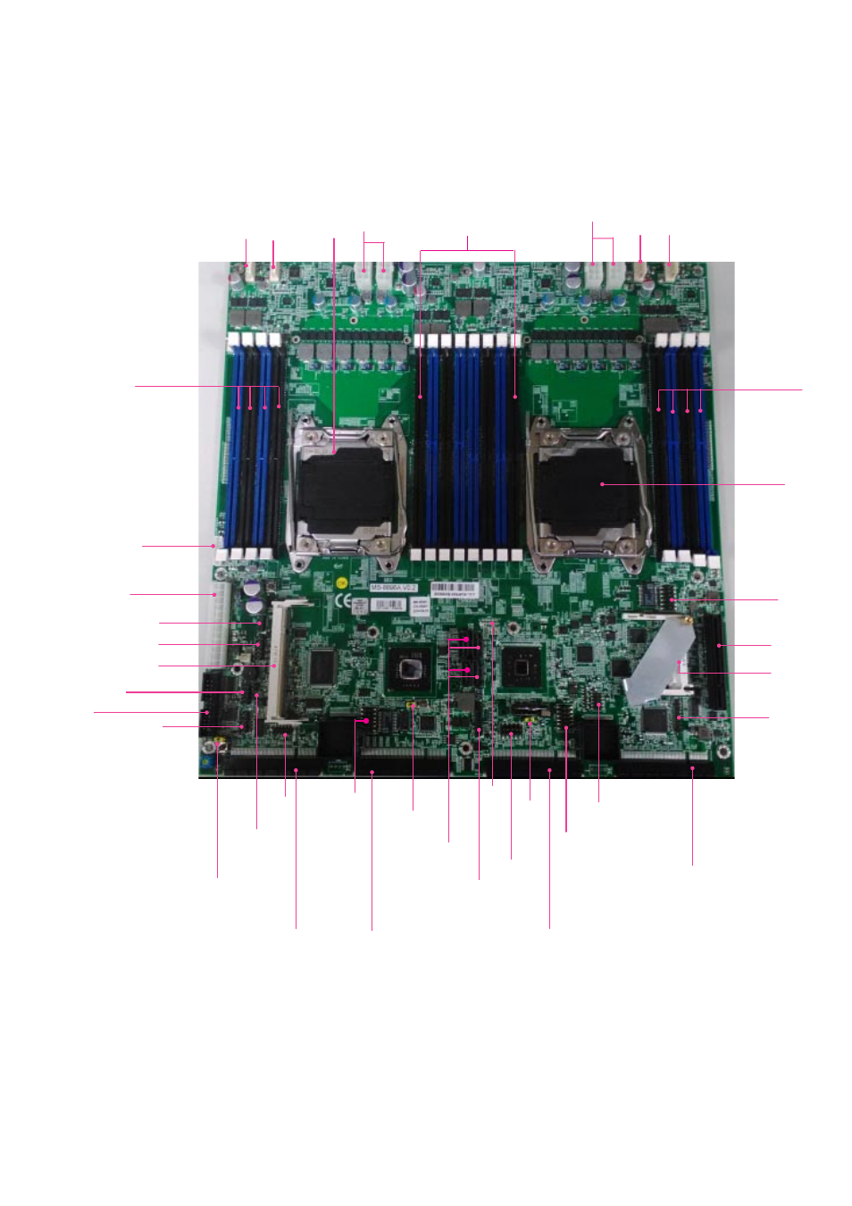
Motherboard Layout
The motherboard layout shows the connectors and
jumpers on the board. Refer to the following picture
as a reference of the pin assignments and the internal
connectors.
CFast1
COMB1
JDDR0-3
MGT1
JFAN2
JDDR12-15
CPU Socket
No.1
JVGA1
MGT2
JCOMA1
JOPMA1
J23
JFAN1
JFAN3 JFAN4
ATX3-4
ATX1-2
CPU Socket NO. 2
JLCM1
JUSB2
JUSB1
ATX5
CON3
SATA1-4
OPEN2
JOPEN1
JDDR4-11
J25
JSPIROM1
JTPM1
J80PORT1
JCMOS
J27
JGP1
JRISER1
JPCIESL4
JPCIESL3
JPCIESL2
JPCIESL1
See also other documents in the category Lanner Computer hardware:
- LVC-2000 (39 pages)
- LVC-5000(N4) (42 pages)
- LVC-5550S (41 pages)
- LVC-5570 (48 pages)
- LVC-5770 (49 pages)
- FW-6432 (16 pages)
- FW-7525 (41 pages)
- FW-5330 (38 pages)
- FW-6486 (18 pages)
- FW-6436 (19 pages)
- FW-7573 (44 pages)
- FW-7568 (52 pages)
- FW-7540 (47 pages)
- FW-8759 (47 pages)
- FW-7581 (23 pages)
- FW-8758 (42 pages)
- FW-7610 (44 pages)
- FW-8756 (24 pages)
- FW-7575 (48 pages)
- FW-8760 (53 pages)
- FW-8877 (46 pages)
- FW-8892 (58 pages)
- FW-8893C (49 pages)
- FX-3411 (48 pages)
- FW-8771 (47 pages)
- RS12-38800 (64 pages)
- MR-320 (20 pages)
- FX-3210 (54 pages)
- MR-301 (16 pages)
- MR-350 (12 pages)
- MR-330A (16 pages)
- MR-730 (18 pages)
- VES-220 (19 pages)
- VES-270 (19 pages)
- VES-310 (15 pages)
- VES-310 V2 (20 pages)
- VES-500 (21 pages)
- EM-F345 (30 pages)
- VES-8X2 (16 pages)
- VES-8X6 (17 pages)
- LEC-2026 (67 pages)
- LEC-2010 (65 pages)
- LEC-2136 (20 pages)
- LEC-2050 (38 pages)