Chapter 2, System components, Block diagram: the mainboard – Lanner LVC-5000(N4) User Manual
Page 8: Intel, Hm65

8
System Components
Chapter 2
Embedded and Industrial Computing
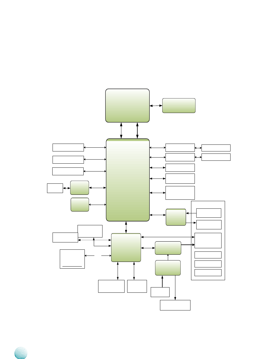
Block Diagram: The MainBoard
The block diagram depicts the relationships among the
interfaces and modules on the motherboard.
Multiple I/O
DVI-D
VGA
Up to 2048X1536@60Hz
HDMI
Up to 1920X1200@75Hz
DVI-D
Up to 1920X1200@75Hz
Intel
HM65
CPU
Sandy Bridge
Fintek
F81865
H/W Monitor
WDT
Digital I/O
(4 D_in & 4 DO)
PS/2 KB/MS
Pin Header
SATA
GbE LAN
4x Intel
82583V
4x PCIe 1X
DDR3
SO-DIMM
(up to 8GB)
Mini PCI Express
Socket
PCIe x1
SIM Card Reader
Serial Port
1x RS232
DB9
4x RJ-45
SATA-III
1x Connector
Compact Flash
Socket
LP
C
SPI Flash
64Mbit
SPI
D
M
I
USB 2.0
USB 2.0 Ports
4x Type A
2x Pin Header
HD Audio
Realtek
ALC886
HD Audio
MIC/Line In
(via MIO)
Audio/Line Out
(via MIO)
UART x 2
UART
Ignition
Controller
LPC1114FHM33/302
PWM
DC-in
+9V~36V
+12V/V
core
/V
io
/V
sb
UART
GPS Receiver
U-blox
NEO-6Q GPS
Mini PCI Express
Socket
PCIe x1
SIM Card Reader
F
D
I
VGA
HDMI
Serial Port
(1x RS232/422/485)
DB9
Relay x 2
MCU control
