Chapter 3, Board layout – Lanner LVC-5000(N4) User Manual
Page 21
21
Board Layout
Chapter 3
Embedded and Industrial Computing
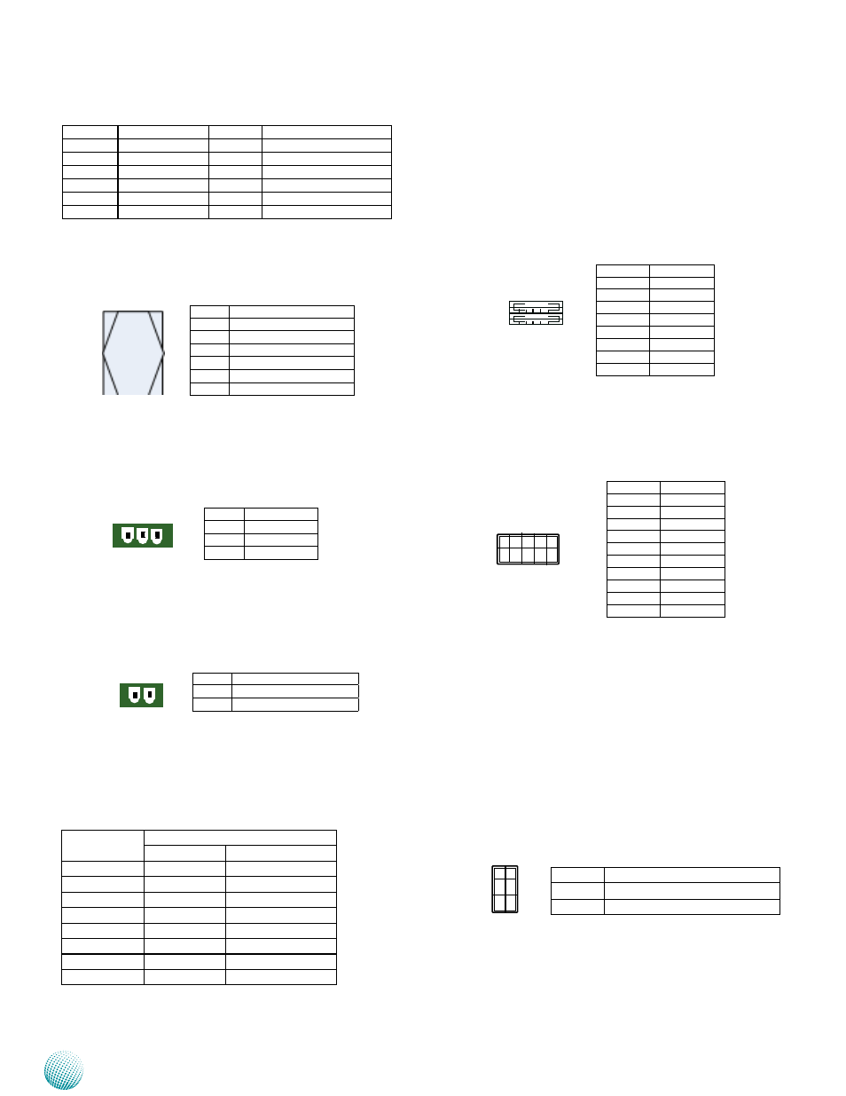
Dual USB 2.0 Port Connector #0 and #1 (USBB1)
Dual USB 2.0 Port Connector #2 and #3 (USBB2)
To erase the CMOS data:
Turn off the computer and unplug the power cord.
Move the jumper cap from pins 1-3 to pins 3-5. Keep
1.
the cap on pins 3-5(4-6) for about 5-10 seconds, then
move the cap back to pins 1-2.
Plug the power cord and turn on the computer.
2.
Enter BIOS setup to re-enter data.
3.
SIM Card Socket (SIM1/SIM2): SIM1 pairs with MPCIE1
and SIM2 pairs with MPCIE2.
Power-in with Ignition Control (PRJK1): A power
connector with power -ignition Control
Distant Power on/off Control (CN3)
LAN1~4 Ports (LANB1~LANB4): The LAN ports are
provided by Intel 82583V Ethernet controller whose
interface complies with PCI-e 1.1 (2.5 Ghz). It is capable of
PXE remote boot.
Pin No.
Description
Fast Ethernet Gigabit Ethernet
1
TX+
BI_DA+
2
TX-
BI_DA-
3
RX+
BI_DB+
4
--
BI_DC+
5
--
BI_DC-
6
RX-
BI_DB-
7
--
BI_DD+
8
--
BI_DD-
Pin No.
Pin Name
1
Ignition
2
GND
3
DC_VIN
1 2 3
1 2 3 4
5 6 7 8
Pin No.
Pin Name
1
VCCUSB
2
USB0N
3
USB0P
4
GND
5
VCCUSB1
6
USB1N
7
USB1P
8
GND
Pin No.
Pin Name
1-3
Normal (Default)
3-5
Clear CMOS
Pin No.
Description
C1
UIM_PWR/UIM2_PWR
C2
UIM_RST/UIM2_RST
C3
UIM_CLK/UIM2_CLK
C5
GND/GND
C6
UIM_VPP/UIM2_VPP
C7
UIM_DAT/UIM2_DAT
C5 C7
C1 C3
6
4
2
Pin No.
Pin Name
1
VCC5
2
GND
3
N/A
4
USBD11P
5
USBD10N
6
USBD11N
7
USBD10P
8
N/A
9
GND
10
VCC5
10 8 6 4 2
9 7 5 3 1
2 1
Pin No.
Pin Name
1
Remote_Power_on
2
GND
Pin
Signal
Pin
Signal
41
VCC3P3_PS
42
LED_WWAN2-
43
GND
44
LED_WLAN2-
45
RSV
46
N/A
47
RSV
48
V1P5_MPCIE
49
RSV
50
GND
51
RSV
52
VCC3P3_PS
5
3
1