Functional description, Input and ancillary data processing – Grass Valley 8990ARC v.1.0 User Manual
Page 26
20
8990ARC Instruction Manual
8990ARC SD Aspect Ratio Converter
Functional Description
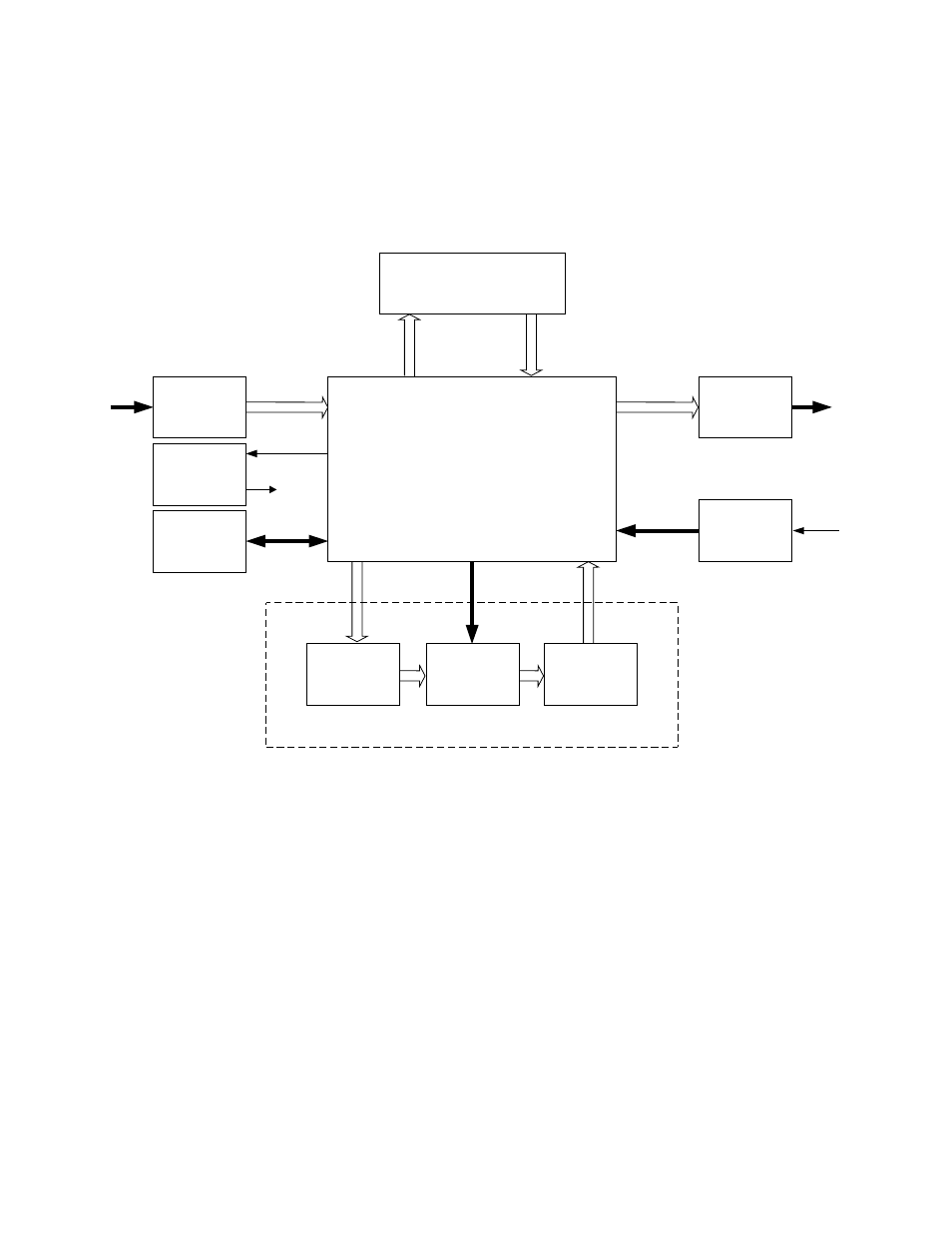
Refer to the block diagram in
while reading the following func-
tional description.
Figure 15. 8990ARC Block Diagram
Input and Ancillary Data Processing
The input signal is deserialized and enters the control Field Programmable
Gate Array (FPGA). Sync is detected and is used to H-lock the system 27
MHz clock. All horizontal and vertical interval data is routed through the
ancillary date (ANC) bypass FIFO to delay match the re-sized active
picture data and is multiplexed back, with the re-sized data, to the parallel
data output. This output is serialized and output through 4 buffers and
connectors.
270 Mb input
270 Mb
Output
ANC Bypass
H & V re-size processing
Processor
and
Power
27 MHz clock
and PLL
27MHz
input h-lock
Processor I/F and Control FPGA
Coefficient loading
and control
GPI Input A/D
Input Y & C
FIFOs
Output Y & C
FIFOs
Horiz & Vert
Polyphase
Filter
- LDK 5302 (24 pages)
- SFP Optical Converters (18 pages)
- 2000GEN (22 pages)
- 2011RDA (28 pages)
- 2010RDA-16 (28 pages)
- 2000NET v3.2.2 (72 pages)
- 2000NET v3.1 (68 pages)
- 2020DAC D-To-A (30 pages)
- 2000NET v4.0.0 (92 pages)
- 2020ADC A-To-D (32 pages)
- 2030RDA (36 pages)
- 2031RDA-SM (38 pages)
- 2041EDA (20 pages)
- 2040RDA (24 pages)
- 2041RDA (24 pages)
- 2042EDA (26 pages)
- 2090MDC (30 pages)
- 2040RDA-FR (52 pages)
- LDK 4021 (22 pages)
- 3DX-3901 (38 pages)
- LDK 4420 (82 pages)
- LDK 5307 (40 pages)
- Maestro Master Control Installation v.1.5.1 (455 pages)
- Maestro Master Control Installation v.1.5.1 (428 pages)
- 7600REF Installation (16 pages)
- 7600REF (84 pages)
- 8900FSS (18 pages)
- 8900GEN-SM (50 pages)
- 8900NET v.4.3.0 (108 pages)
- Safety Summary (17 pages)
- 8900NET v.4.0.0 (94 pages)
- 8906 (34 pages)
- 8911 (16 pages)
- 8900NET v.3.2.2 (78 pages)
- 8914 (18 pages)
- 8912RDA-D (20 pages)
- 8916 (26 pages)
- 8910ADA-SR (58 pages)
- 8920ADC v.2.0 (28 pages)
- 8920ADC v.2.0.1A (40 pages)
- 8920DAC (28 pages)
- 8920DMX (30 pages)
- 8920ADT (36 pages)
- 8920MUX (50 pages)
- 8921ADT (58 pages)